Modern electronics continue to evolve toward higher performance, greater functionality, and smaller form factors. This trend places increasing demands on printed circuit board (PCB) design, where more complex circuits must be integrated into increasingly limited space. Conventional multilayer PCB fabrication remains widely used, but it faces growing challenges in supporting ultra-fine routing, high interconnect density, and advanced packaging requirements.
Sequential Build-Up (SBU) technology was introduced to address these challenges and has become a core process in High-Density Interconnect (HDI) PCB manufacturing. Unlike conventional methods that laminate multiple layers in a single cycle, SBU builds the PCB structure step by step by adding dielectric and copper layers sequentially onto a core substrate. This approach enables finer features, smaller vias, and significantly higher wiring density.
However, the advantages of SBU come with increased process complexity. Each build-up stage involves multiple critical steps, including dielectric deposition, laser drilling (microvias), metallization, and plating. Variations at any stage can accumulate and affect overall yield and long-term reliability.
Achieving stable manufacturing performance requires a deep understanding of process interactions, tight control of critical parameters, and effective strategies for managing variation across each build-up cycle.
In this article, we focus on one of the most critical factors affecting SBU performance: microvia reliability and manufacturing yield stability. We will also introduce a practical framework to help engineers analyze root causes, control process variation, and improve overall yield and reliability in HDI PCB fabrication.
The growing adoption of Sequential Build-Up PCB technology is primarily driven by the increasing complexity of modern electronic systems.
Advanced packaging technologies such as ball grid arrays (BGAs), chip-scale packages (CSPs), and flip-chip devices feature extremely fine pitches and dense I/O configurations. Routing signals out from beneath these components—commonly referred to as “escape routing”—requires significantly higher interconnect density than what conventional multilayer PCB designs can efficiently support.
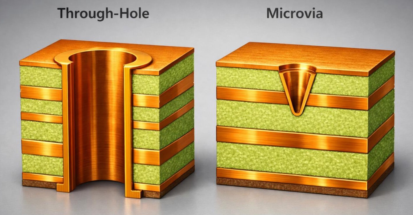
Traditional multilayer PCB rely heavily on mechanically drilled through-holes. While robust and cost-effective, these vias occupy considerable space across all layers and can restrict routing channels. In addition, they introduce electrical challenges such as via stubs, larger parasitic capacitance and inductance, and impedance discontinuities, all of which can negatively impact signal integrity—especially in high-speed designs.
SBU technology addresses these limitations by enabling the use of laser-drilled microvias and sequential layer construction (e.g., 2+1+2 stack-ups). Microvias are much smaller than through-holes and can be placed more precisely, including directly in component pads (via-in-pad). This allows for more efficient escape routing and significantly improves routing density without increasing board size.
From an electrical perspective, SBU also offers important advantages. By reducing via size, shortening interconnect paths, and minimizing parasitic effects, it helps improve signal integrity in high-speed, multi-gigahertz systems. This is particularly important for designs sensitive to signal reflections, impedance mismatches, and electromagnetic crosstalk.
Finally, SBU enables a more optimized layer build-up strategy. Instead of laminating all layers at once, manufacturers can selectively add layers only where needed, which can improve design flexibility and, in some cases, enhance manufacturing efficiency.
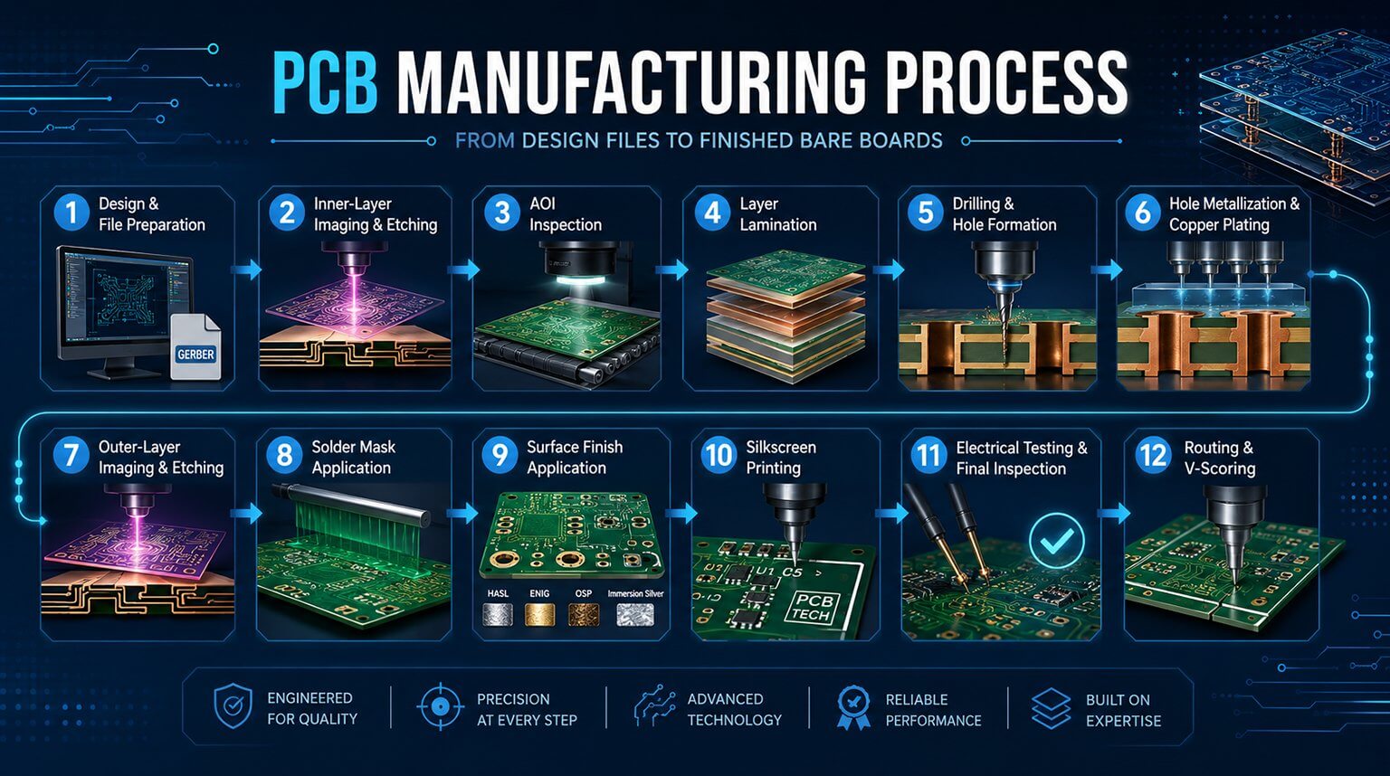
The defining feature of SBU PCB construction is its layer-by-layer fabrication approach. The typical manufacturing process can be described in the following steps:
- Core Substrate Fabrication
The process begins with the fabrication of a core substrate, which serves as the mechanical and electrical foundation of the PCB. This core may include one or more copper layers used for power distribution or signal routing. Standard photolithography and etching processes are used to define circuit patterns, and mechanical drilling is performed to create any required through-holes.
- Dielectric Layer Lamination
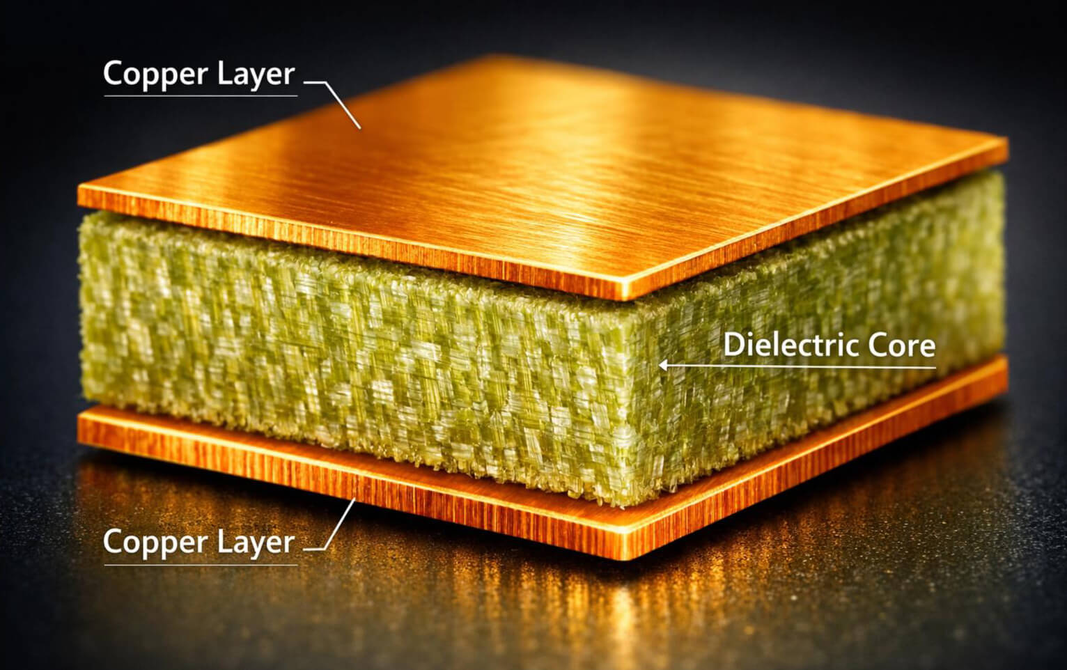
Once the core is completed, a thin dielectric layer is laminated onto its surface. This is typically achieved using resin-coated copper (RCC) or specialized prepreg materials. Compared to conventional multilayer boards, the dielectric used in SBU is significantly thinner, allowing tighter layer spacing.
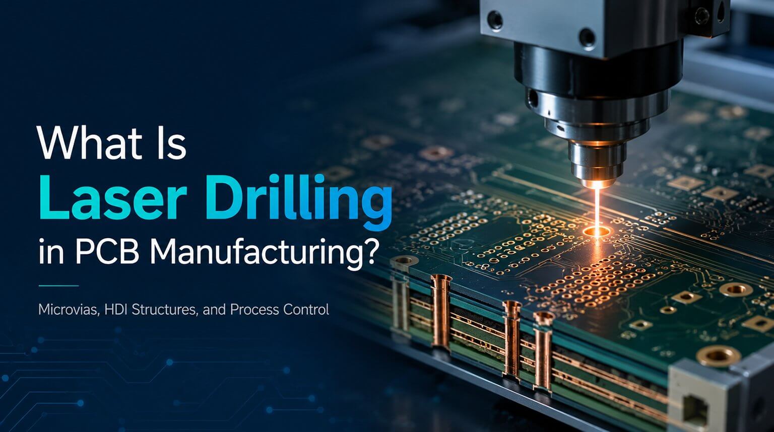
- Laser Drilling of Microvias
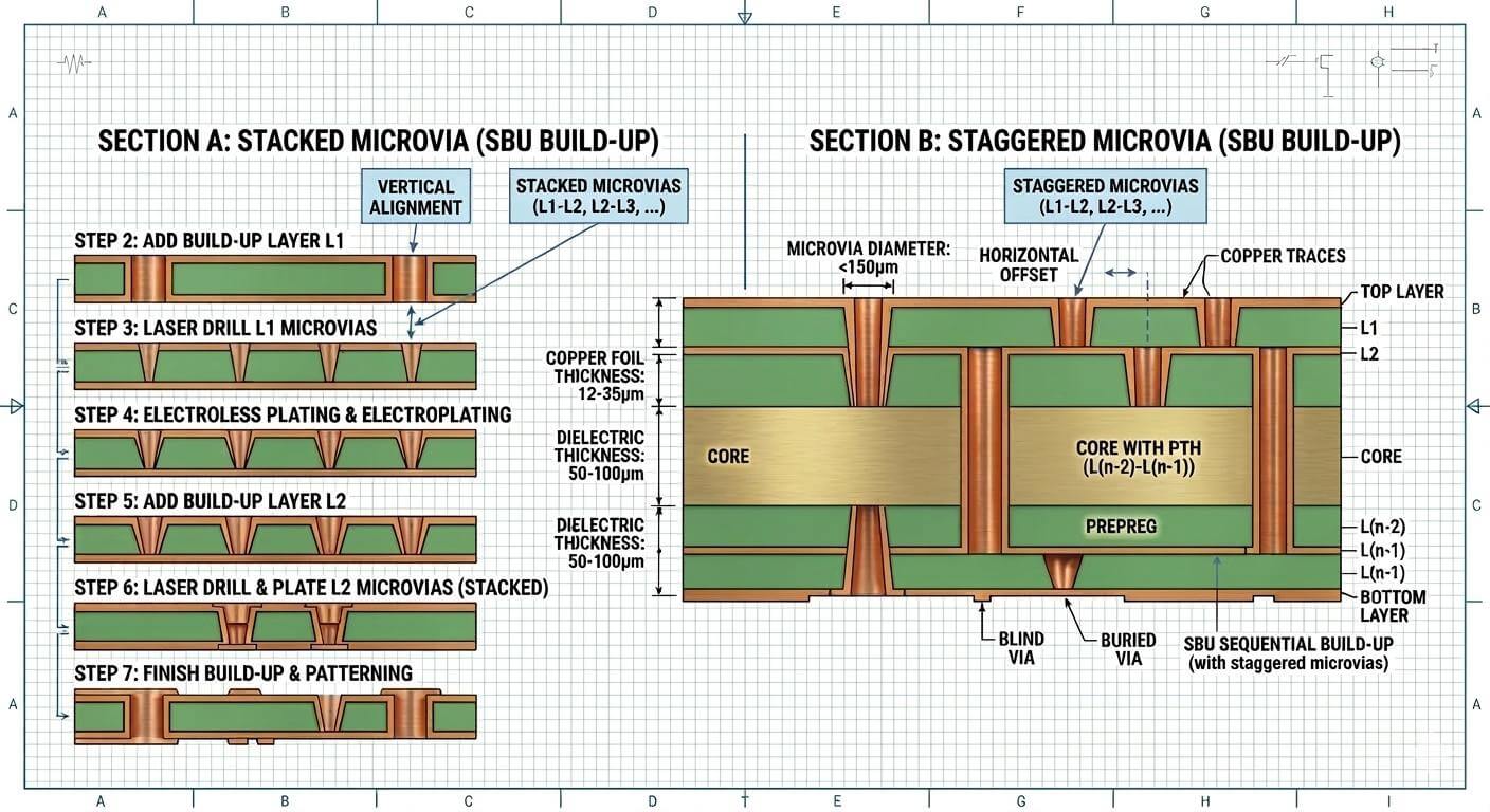
After lamination, microvias are formed using laser drilling. Unlike traditional through-holes, microvias typically connect only adjacent layers (blind vias) rather than passing through the entire board. Their small size—commonly in the range of 50–100 microns in diameter—enables high interconnect density and precise routing in HDI designs.
- Metallization and Copper Plating
The drilled microvias are then metallized. This process begins with the deposition of a thin conductive seed layer (commonly via electroless copper deposition), followed by electroplating to build up sufficient copper thickness. In many designs, microvias are fully or partially copper-filled to create a flat, reliable surface for subsequent layers.
- Pattern Formation
Once the copper layer is established, photolithography and etching processes are used to define the circuit patterns on the newly added layer.
- Sequential Layer Build-Up
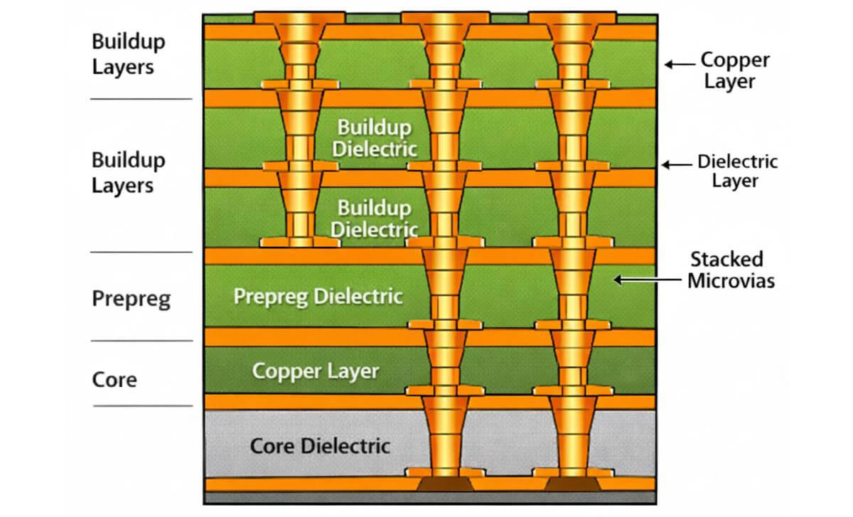
Steps 2 through 5 are repeated as needed to achieve the required number of build-up layers (e.g., 1+N+1, 2+N+2 structures). Each cycle adds additional routing capability and interconnect density, allowing the PCB to meet increasingly complex design requirements.
As discussed previously, microvias are formed after each build-up layer is laminated and are typically very small in size. In multi-layer sequential lamination structures, microvias can be arranged in two primary configurations: stacked (vertically aligned) or staggered (offset between layers).
Stacked microvias offer clear advantages in terms of space utilization and routing efficiency, especially in high-density designs. However, they also introduce greater reliability risks compared to staggered structures, particularly under thermal and mechanical stress. As a result, stacked microvias are often considered one of the most critical challenges in SBU PCB manufacturing.
During production, manufacturers may encounter several types of microvia-related defects:
- Barrel cracking after thermal cycling
- Copper separation between stacked microvias
- Intermittent electrical connections during testing
- Reduced manufacturing yield due to interconnect defects
- Field failures in high-reliability applications such as automotive and aerospace systems
These failures typically do not occur as isolated events. Instead, they are often the result of accumulated stress introduced during repeated lamination, drilling, and plating cycles. Differences in material properties, thermal expansion mismatch, and process variations can all contribute to the degradation of microvia integrity over time.
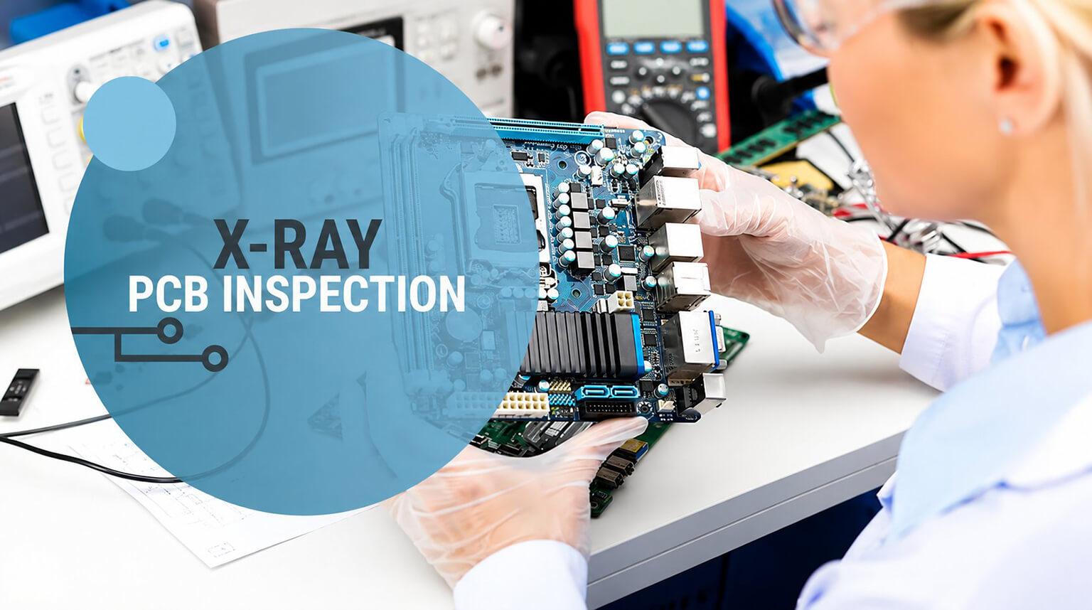
For high-volume manufacturing, even a small increase in microvia defect rates can have a significant impact on overall yield and production cost. Boards that fail during assembly or environmental testing often require destructive analysis techniques—such as cross-sectioning—to identify the root cause of failure.
All materials used in PCB construction expand when heated and contract when cooled. However, each material—such as laminate substrates, copper foil, dielectric layers, and resin systems—has its own coefficient of thermal expansion (CTE).
During thermal processes such as lamination and solder reflow (typically exceeding 240 °C), these materials expand at different rates. This mismatch generates mechanical stress within the microvia structure. When repeated over multiple thermal cycles, the accumulated stress can exceed the mechanical limits of the plated copper, leading to crack initiation in the microvia barrel or at the interfaces of stacked microvias.
This issue is further intensified by the anisotropic nature of PCB materials. Expansion in the Z-axis (thickness direction) is typically much greater than in the X–Y plane. During reflow, dielectric materials tend to expand more in the Z-direction than copper, placing additional tensile stress on the microvia structure. Over time, cyclic thermal loading leads to copper fatigue and eventual failure.
The quality and uniformity of copper plating inside microvias are critical to ensuring reliable electrical interconnections. The plated copper must withstand thermal, mechanical, and electrical stresses throughout the product lifecycle.
Several factors can lead to inconsistent plating:
- Non-uniform current distribution during electroplating
- Contamination in the plating bath chemistry
- Inadequate solution circulation or agitation
- Incorrect plating parameters (e.g., current density, time, temperature)
Poor plating uniformity can result in localized thin copper regions within the microvia barrel. These areas are more susceptible to increased current density and thermal stress during operation, which accelerates fatigue and increases the risk of cracking.
Laser drilling is the standard method for forming microvias in SBU processes due to its high precision. However, improper process control can introduce defects that compromise reliability.
Common issues include:
- Residual carbon or debris from incomplete dielectric ablation
- Rough via sidewalls that reduce copper adhesion
- Incomplete cleaning of drilling residues
- Damage to underlying copper pads (target pad damage)
Any contamination or surface irregularity inside the microvia can weaken the adhesion between the copper plating and the dielectric material, increasing the likelihood of delamination or cracking under stress.
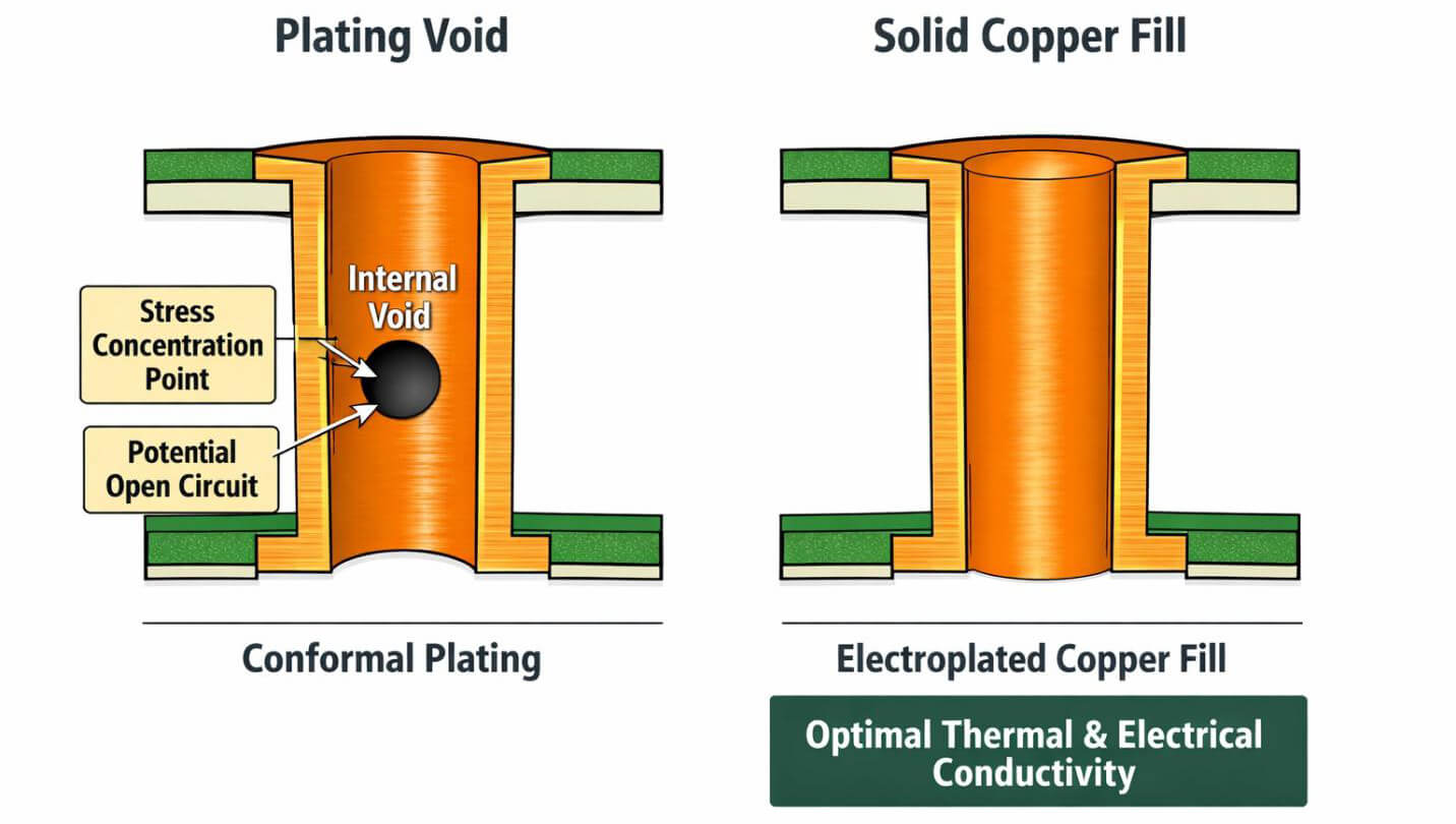
During the lamination process, resin must flow uniformly around copper features and fill all gaps. Insufficient or uneven resin flow can lead to void formation, particularly around microvia pads.
These voids act as stress concentration points. Under thermal cycling, stress tends to accumulate around these regions, accelerating crack initiation and propagation. Over time, this can significantly reduce the mechanical reliability of the microvia structure.
Stacked microvia structures enable high-density vertical interconnections but also introduce increased mechanical stress concentration. Each additional stacked layer compounds the stress experienced during thermal cycling.
As stress accumulates through repeated expansion and contraction cycles, the copper interfaces within the stacked vias become more prone to fatigue. This can lead to crack formation, interfacial separation, and eventual electrical failure.
Because multiple lamination and thermal cycles are involved, material compatibility is critical to minimizing internal stress.
Key material characteristics include:
- Low coefficient of thermal expansion (CTE), especially in the Z-axis
- High glass transition temperature (Tg)
- Stable and consistent resin flow behavior
- Proven compatibility with multiple lamination cycles
Materials specifically engineered for HDI applications—such as resin-coated copper (RCC) and advanced build-up films—offer better thickness control and more predictable processing performance.
Microvia geometry directly affects plating quality, stress distribution, and long-term performance.
Common design guidelines include:
- Microvia diameter typically in the range of 50–100 µm (depending on capability)
- Aspect ratio generally below ~0.75 for reliable plating
- Sufficient capture pad size to ensure proper alignment and connection
- Limiting the number of stacked microvia layers where possible
Whenever feasible, staggered microvia configurations are preferred over fully stacked structures. Staggered designs help distribute mechanical stress more evenly across layers, reducing the risk of fatigue failure.
Poorly controlled drilling can introduce defects that weaken metallization and reduce adhesion.
Critical process parameters include:
- Laser pulse energy and frequency
- Focus position relative to dielectric thickness
- Drilling speed and consistency
- Effective removal of debris during drilling
Post-drilling treatments—such as plasma cleaning or chemical desmear—are commonly used to remove carbon residues and improve copper adhesion. Proper surface preparation is essential for achieving reliable metallization.
Advanced plating techniques, such as pulse plating, are often used to improve copper distribution, especially in high aspect ratio features. This approach helps reduce void formation and ensures more uniform thickness along the via walls.
Additional process controls include:
- Continuous monitoring of plating bath chemistry
- Optimized electrolyte flow and agitation
- Automated control of additives and replenishment systems
Maintaining plating uniformity minimizes localized weak points and reduces the risk of fatigue cracking under thermal and electrical stress.
Each lamination cycle introduces thermal and mechanical stress into the PCB structure. Poorly controlled thermal profiles can accelerate material degradation and increase the likelihood of microvia failure.
Effective lamination control involves:
- Controlled heating ramp rates
- Uniform pressure distribution across the panel
- Optimized dwell time at peak temperature
- Gradual and controlled cooling cycles
In advanced manufacturing environments, process simulation tools are often used to predict stress accumulation and optimize lamination parameters before production. This helps reduce trial-and-error and improves overall process stability.
A telecommunications equipment manufacturer was developing a 12-layer HDI PCB for high-speed networking applications. The design utilized a typical SBU structure, with two build-up layers added on each side of the core (commonly referred to as a 2+N+2 stack-up), incorporating stacked microvias to achieve the required routing density.
During early-stage production, intermittent failures were observed during electrical testing. Initial inspection did not reveal obvious defects, but cross-sectional analysis identified cracking in microvias located within the second build-up layer.
At first, the issue was suspected to be related to insufficient copper plating within the microvias. However, plating thickness measurements confirmed that the process was within specification.
Further investigation revealed that the primary cause was a mismatch in Z-axis coefficient of thermal expansion (CTE) between the build-up dielectric material and the core laminate. During solder reflow, this mismatch generated significant mechanical stress, particularly in the stacked microvia structures. The stress concentration led to fatigue cracking in the microvia interfaces.
To address the issue, the engineering team applied a structured reliability improvement approach based on the Sequential Reliability Control Framework. The following actions were implemented:
- Material optimization: Replaced the build-up dielectric with a material offering better thermal compatibility with the core laminate
- Design improvement: Reduced the number of stacked microvias and introduced staggered via structures in critical areas
- Process refinement: Optimized laser drilling parameters to improve via wall quality
- Surface preparation enhancement: Added plasma cleaning prior to metallization to improve copper adhesion
Following these improvements, manufacturing yield increased significantly, and intermittent electrical failures were eliminated. Subsequent thermal cycling tests confirmed that the revised structure provided stable and reliable performance under stress conditions.
As electronic systems continue to evolve toward higher speeds, greater functionality, and increased integration density, the role of Sequential Build-Up (SBU) technology in PCB manufacturing will only become more critical. SBU enables the high-density interconnect structures required by modern designs, but it also introduces new challenges in reliability, process control, and material compatibility.
Successfully implementing SBU technology is not solely a matter of advanced fabrication capability—it requires a comprehensive understanding of materials, microvia design, and tightly controlled manufacturing processes. Engineers and manufacturers who adopt systematic reliability control strategies will be better positioned to deliver HDI PCB that meet the demanding performance and durability requirements of next-generation applications.
Bei PCBCool, we specialize in high-reliability HDI and Sequential Build-Up PCB manufacturing, supporting both prototype and volume production.
We provide:
- Advanced SBU structures (1+N+1, 2+N+2, and complex any-layer stack-ups)
- High-precision laser-drilled microvias (including stacked and staggered designs)
- Strict process control for plating, lamination, and material compatibility
- Engineering support for DFM optimization and reliability improvement
- Rapid prototyping services, with support for complex HDI builds
Whether you are developing high-speed communication systems, industrial electronics, or next-generation embedded devices, PCBCool is your trusted HDI PCB manufacturing partner, helping you optimize designs for manufacturability, improve yield, and ensure long-term reliability.