Imagine this: You’ve spent weeks (or months) designing your dream PCB, maybe a custom IoT sensor for Lagos traffic monitoring, a solar charger prototype, or your final-year project. You export the files, upload them to your favorite fab house (PCBCool, RushPCB, or a local service), hit “order,” and wait excitedly for the boards to arrive.
Then the email comes: “Production on hold, issues detected in your files.” Or worse, the boards show up… but they’re unusable. Holes in the wrong places, missing solder mask, components that won’t fit, or entire layers ignored. Your project stalls, deadlines slip, and that small budget for prototypes suddenly balloons with re-orders, rework, or worse, starting over.
This isn’t rare. In 2025–2026, even with advanced online tools and auto-checkers, wrong or incomplete files remain one of the top reasons PCB orders get delayed, rejected, or returned.
Common pain points include:
- Missing or mismatched layers in Gerbers → boards fabricated without copper tracks, solder mask, or silkscreen.
- Drill file errors (wrong sizes, missing holes, or plated vs non-plated mix-ups) → vias don’t connect, through-hole parts can’t mount.
- BOM mistakes (outdated part numbers, wrong footprints, missing quantities) → wrong components sourced, assembly halted.
- Pick-and-place file issues → robots place parts rotated 180°, off-center, or not at all.
- No clear instructions (stack-up, finish, colors) → you get HASL when you needed ENIG, or green mask instead of black.
These slip-ups cause delays of days to weeks (waiting for engineering queries or file fixes), extra costs (re-fabrication fees, expedited shipping, wasted components), and frustration, especially when you’re in a rush or learning the process for the first time.
The good news? Almost every issue is preventable with the right preparation. This guide walks you through every essential file needed for a successful bare-board fabrication and full PCBA (assembly), from Gerbers to BOMs and beyond. By the end, you’ll know exactly what to generate, how to verify it, and what modern options (like ODB++ or IPC-2581) can simplify everything.
Whether you’re using KiCad in a Lagos makerspace, EasyEDA online, or Altium at work, getting the files right the first time saves time, money, and headaches. Let’s dive in.
Understanding the difference between PCB fabrication and PCB assembly is essential before preparing files. These are two separate stages in turning your design into a working board.
PCB fabrication produces the bare board (also called PCB or printed circuit board). This stage creates the physical structure: copper layers, substrate, solder mask, silkscreen, and drilled holes. No components are added yet. The factory uses your Gerber files, drill files, and mechanical drawings to etch copper, apply a mask, and cut the board to shape. The output is an empty board ready for population.
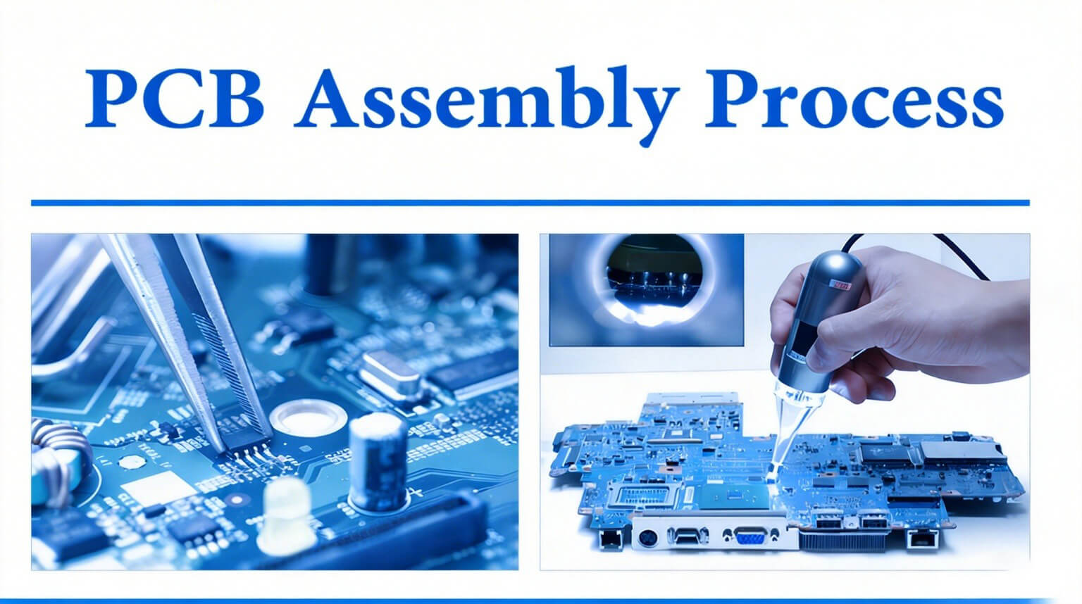
PCB assembly (or PCBA) adds components to the bare board to make it functional. This includes soldering resistors, capacitors, ICs, connectors, and other parts. Assembly requires additional files like the BOM (Bill of Materials) and pick-and-place (centroid or XY) file. The factory or assembler sources parts, applies solder paste, places components with machines, and sells them (usually via reflow). The final result is a fully populated, testable board.
Many people order bare boards only (fabrication) when prototyping or testing. For full turnkey service, they order PCBA (fabrication + assembly).
Knowing the difference helps you decide which files to send and what to specify. Here is a quick comparison:
Fabrication (Bare Board)
- Goal: Create the empty PCB
- Key files: Gerbers, NC drill, fabrication drawing
- Ausgabe Board with traces, pads, mask, legend (no parts)
- Common for: Prototyping, low-volume, or when you assemble yourself
Assembly (PCBA)
- Goal: Populate the board with components
- Key files: BOM, pick-and-place file, assembly drawing
- Ausgabe Functional board with soldered components
- Common for: Production, when outsourcing full build
Most online fabs offer both services separately or together. Always confirm with your manufacturer what they need for each stage.
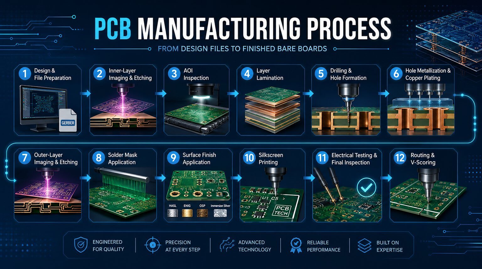
The bare board fabrication files tell the manufacturer how to build the empty PCB — the physical substrate with copper traces, holes, protective coatings, and markings. These files are the core requirement for any PCB order, even if you plan to assemble the board yourself later.
Without correct fabrication files, the factory cannot produce the board accurately. Missing or corrupted files often lead to rejected orders or boards that do not match your design.
Here are the three main file groups required for bare board fabrication:
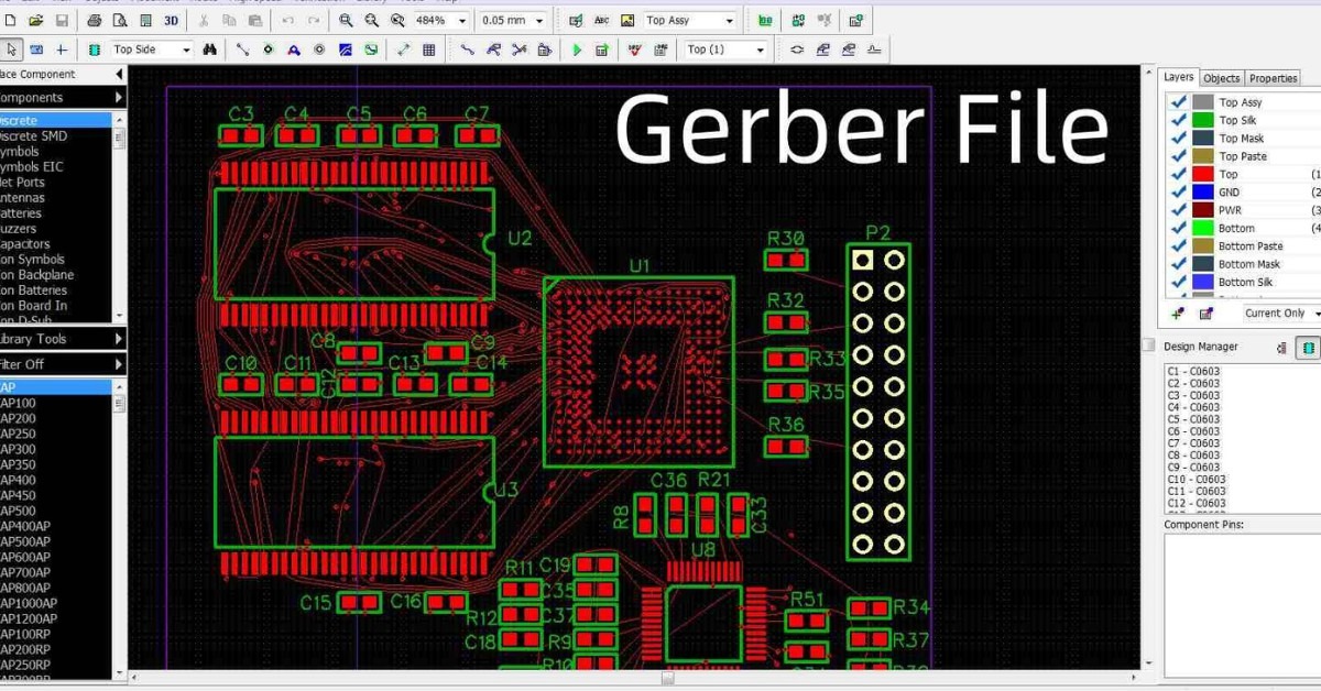
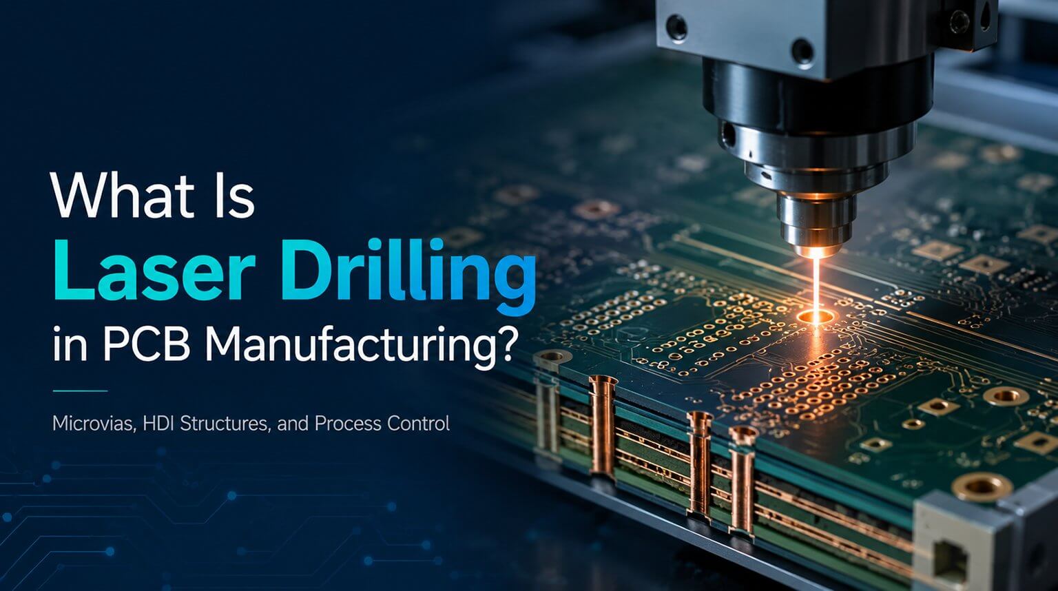
Gerber files (RS-274X format) are the industry standard for describing every layer and feature of the PCB. Each file represents one specific layer or purpose.
Common Gerber files include:
- Top copper layer (.GTL or TopCopper.gbr): conductive tracks on the top side
- Bottom copper layer (.GBL or BotCopper.gbr): conductive tracks on the bottom side
- Top solder mask (.GTS or TopMask.gbr): green (or other color) protective coating on top, openings for pads
- Bottom solder mask (.GBS or BotMask.gbr): same for bottom side
- Top silkscreen/legend (.GTO or TopSilk.gbr): white text, logos, component labels on top
- Bottom silkscreen (.GBO or BotSilk.gbr): same for bottom (often optional if single-sided)
- Board outline (.GML, .GM1, or Outline.gbr): defines the exact shape and cutouts of the board
- Solder paste layers (.GTP / .GBP for top/bottom): used for stencil creation if assembling later
Für multi-layer boards, additional inner copper layers appear (e.g., .G1, .G2 for layers 2 and 3). Always include all relevant layers from your design tool.
Gerber files are usually exported as a zip archive containing 8–12 individual files.
These images show a typical set of Gerber layers: separate views for top copper (red), bottom copper (blue/green), solder mask, and silkscreen overlaid.
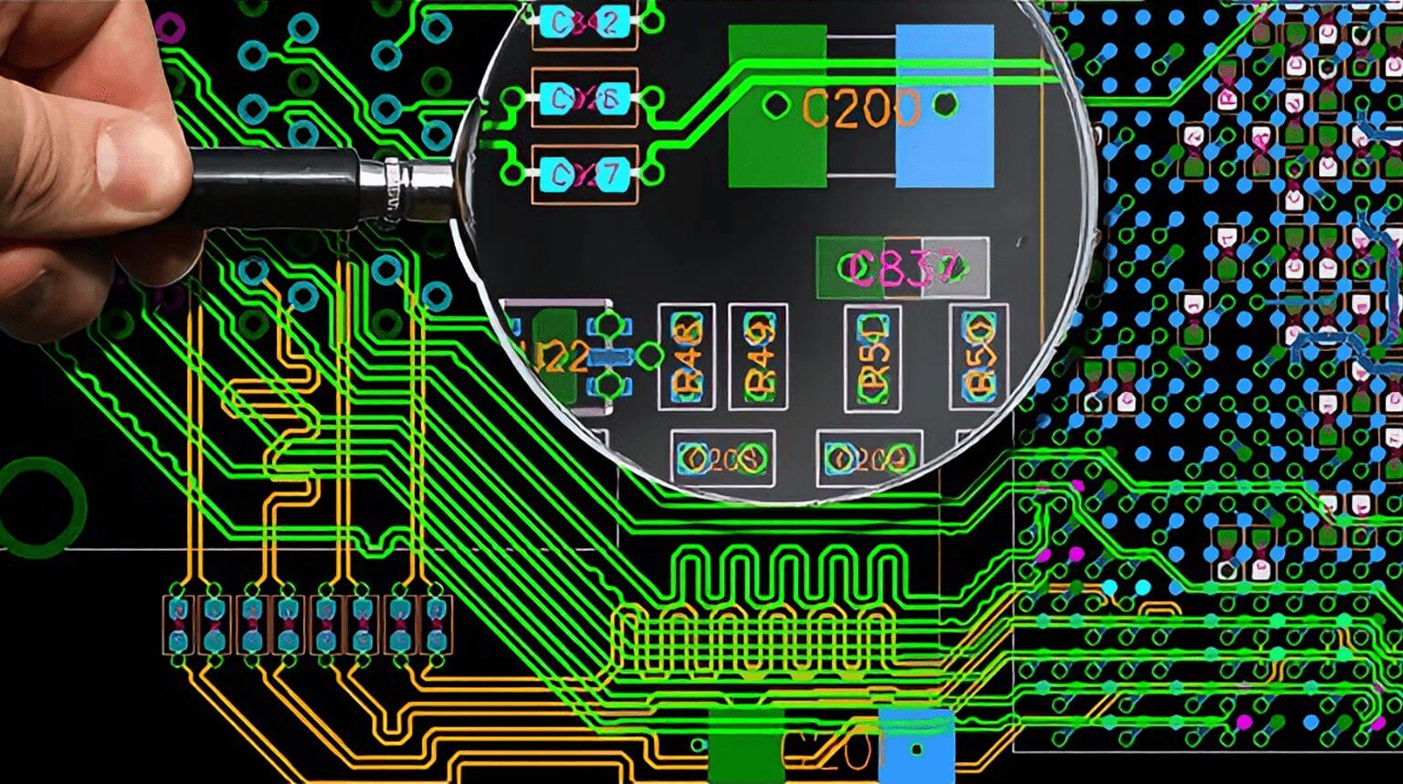
NC Drill files specify every hole location, size, and type (plated or non-plated).
- Plated through-holes and vias connect layers electrically
- Non-plated holes are for mechanical mounting or slots
Typical files:
- One combined file (often .drl) for all plated holes
- Separate file for non-plated holes if your design has them
The file lists X/Y coordinates and tool diameters (e.g., 0.3 mm via, 1.0 mm mounting hole). These show plated through-hole vias (copper-plated inside) versus non-plated mechanical holes.
Errors here (wrong sizes or missing holes) prevent proper connectivity or component fit. Always generate both plated and non-plated if applicable.
A fabrication drawing is a clear PDF document with instructions that Gerber cannot convey.
It typically includes:
- Board dimensions and outline tolerances
- Layer stack-up (material thicknesses, copper weights, total board thickness)
- Surface finish (HASL, ENIG, OSP)
- Solder mask and silkscreen color
- Any special requirements (impedance control, via filling, beveling)
- Notes on V-scoring, tab routing, or panelization
- Fiducial marks location if needed
- Title block with revision, date, and designer info
These examples show detailed stack-up diagrams and mechanical notes with dimensions and tolerances. Even simple 2-layer boards benefit from this file to avoid assumptions by the fab house.
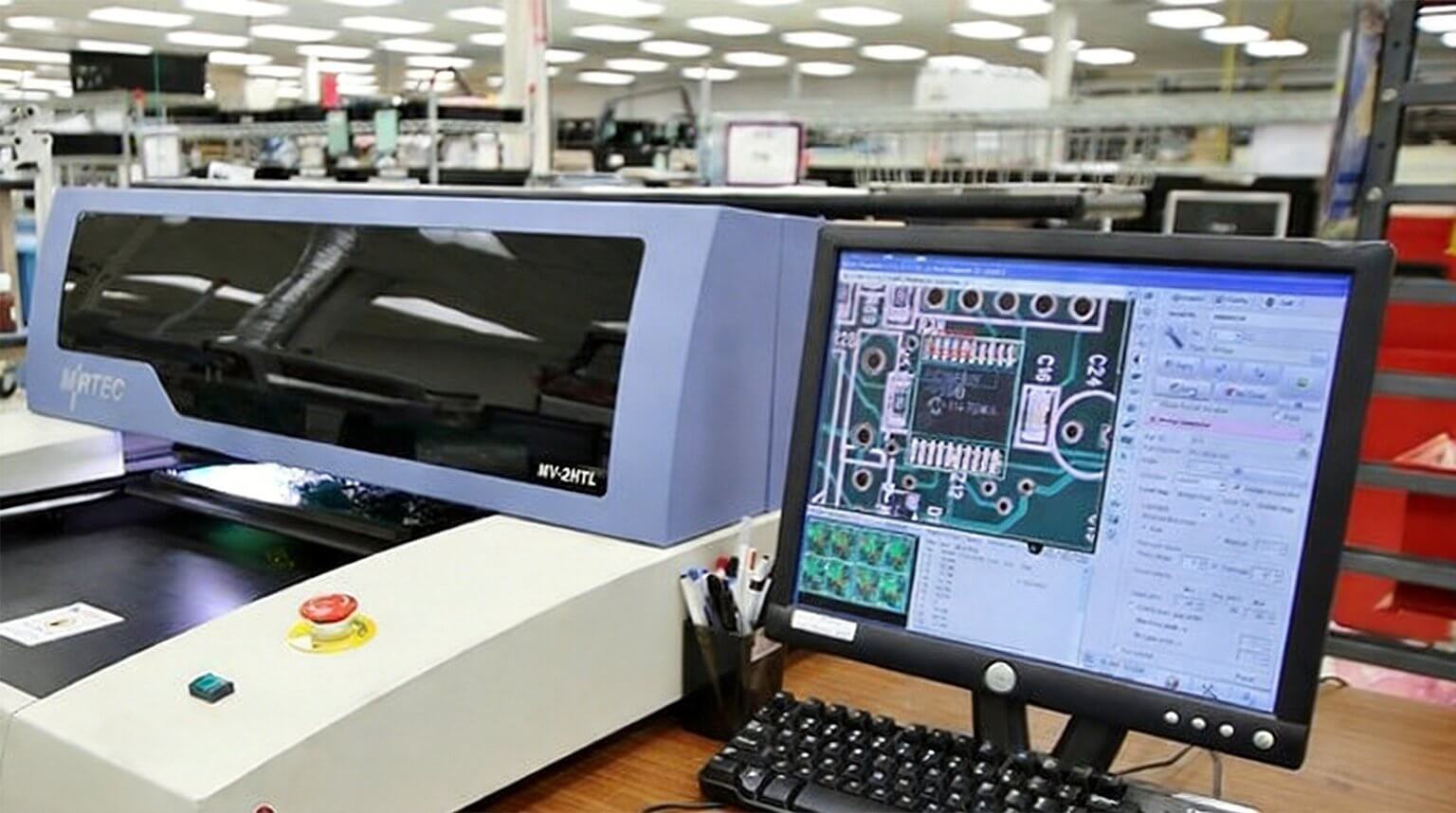
- Use a free Gerber viewer (Gerbv, Tracespace, or online tools) to check all layers before upload.
- Zip all Gerber + drill files together (most fabs prefer one zip).
- Include the fabrication drawing as a separate PDF in the upload.
- Run a full design rule check (DRC) and Gerber preview in your tool before export.
- For advanced options like controlled impedance, specify clearly in the drawing or order notes.
Assembly files are required when you order PCB assembly (PCBA) service, where the manufacturer populates the bare board with components. These files instruct the assembler on which parts to use, their exact locations, orientations, and any additional handling instructions.
Accurate assembly files prevent common issues such as wrong components being installed, parts placed in incorrect positions, wrong rotations, or missing placements altogether. Mistakes here can result in non-functional boards, extra rework charges, or the need to re-order the entire assembly.
Here are the three primary assembly files:
The BOM is a detailed list of every component required on the board. It serves as the sourcing and verification reference for the assembler.
Recommended format: CSV or XLSX (CSV is widely preferred for compatibility with online fabs).
Key columns to include:
- Designator / Reference (e.g., R1, C3, U2)
- Menge
- Value / Description (e.g., 4.7kΩ resistor, 22µF 16V capacitor)
- Footprint / Package (e.g., 0603, QFN-32)
- Manufacturer Part Number (MPN)
- Manufacturer name
- Optional but helpful: Supplier part number (e.g., LCSC or DigiKey ID), tolerance, voltage/power rating, link to datasheet
Sort entries by reference designator (alphabetical/numerical order) or by value for easier review. Use “DNP” (Do Not Populate) or “NC” (No Connect) for components that should be left empty. Verify part availability early to avoid delays from out-of-stock items.
This file contains precise machine coordinates for automated placement of surface-mount devices (SMD). It directs the pick-and-place equipment on position, rotation, and board side for each component.
Common format: CSV or TXT.
Standard columns:
- Designator (e.g., R1)
- Mid X (center X coordinate, usually in mm)
- Mid Y (center Y coordinate)
- Rotation (in degrees, typically 0, 90, 180, or 270)
- Layer / Side (Top or Bottom)
- Optional: Footprint, comment, or height information
Through-hole components are normally excluded, as they are placed manually. Coordinates must align with the board’s origin point (most tool uses bottom-left corner as 0,0). Always generate this file from your layout tool and confirm the units (mm is standard).
The assembly drawing is a PDF that provides a human-readable visual guide and notes that cannot be fully captured in data files alone.
Typical contents:
- Top-side and bottom-side views showing component outlines with reference designators
- Polarity markings for polarized parts (diodes, LEDs, electrolytic capacitors, IC pin 1 indicators)
- Special instructions (e.g., “hand solder J1”, “apply adhesive here”, “do not wash this area”)
- Locations of test points, fiducials, or stickers
- Any height restrictions or mechanical considerations
- Callouts referencing specific BOM entries or assembly steps
For simple single-sided boards, the silkscreen may be sufficient in some cases. For double-sided or complex designs, a dedicated assembly drawing significantly reduces misinterpretation.
- Export BOM and pick-and-place files directly from your design tool using built-in exporters.
- Upload them separately or bundled in a zip folder along with fabrication files if ordering full PCBA.
- Clearly indicate the top/bottom side for double-sided assemblies.
- Include any special requirements (e.g., lead-free process, specific solder type) in the order notes or assembly drawing.
While traditional Gerber files, NC drill files, BOMs, and pick-and-place files remain the most widely accepted and reliable options in 2026, modern intelligent formats offer a more efficient way to package everything. These alternatives bundle layers, drill data, netlists, stack-up details, assembly information, and more into fewer files. They reduce errors from mismatched or missing separate files, speed up verification, and better preserve design intent.
The two leading modern formats are ODB++ and IPC-2581 (with mentions of Gerber X3 in some contexts). Here is a breakdown of each.
ODB++ (Open Database++) is a structured, intelligent format developed by Valor (now part of Siemens). It organizes all fabrication and some assembly data into a hierarchical directory structure, typically zipped into a single archive file.
Key advantages:
- Comprehensive data in one package: Includes layers, drill information, netlist, stack-up, components, and more
- Reduces interpretation errors: The format keeps design hierarchy and intent intact
- Widely supported in advanced CAM systems and by many high-volume manufacturers
- Good for complex boards with impedance control, embedded components, or panelization
Key disadvantages:
- Proprietary origins (though free to use): Owned by Siemens, which can limit full openness
- Requires compatible tools: Not every free viewer or small fab supports it natively
- Larger file size compared to a single XML file
Many professional workflows and EMS partners prefer ODB++ for its reliability in automated processes. Tools like Altium, KiCad (in recent versions), and others can export ODB++ directly.
IPC-2581 is an open, vendor-neutral standard maintained by the IPC consortium. It uses a single XML-based file (sometimes compressed) to contain all necessary fabrication and assembly data.
Key advantages:
- Fully open and free: No licensing restrictions, promotes interoperability across tools and fabs
- Single file simplicity: Everything from Gerbers-equivalent data to BOM, placement, and notes in one package
- Better future-proofing: Growing adoption in 2025-2026 due to push for open standards and reduced vendor lock-in
- Includes rich metadata: Stack-up, materials, netlist, test points, and assembly instructions
Key disadvantages:
- Adoption still catching up: Not every manufacturer or older CAM system supports it fully yet
- Some tools have export bugs: Early implementations (e.g., in KiCad versions before fixes) had readability issues
- Less universal than Gerber for very basic or low-cost fabs
IPC-2581 gains traction in collaborative, multi-vendor environments and forward-looking projects. Many modern design tools (Altium, Cadence, KiCad 9+, etc.) support export, and leading fabs increasingly accept it.
Gerber X3 is an evolution of the classic Gerber format (mentioned in context), adding assembly and component data (similar to X2 upgrades for attributes). It aims to bridge legacy Gerber with intelligent formats but sees limited standalone use compared to ODB++ or IPC-2581.
- Use ODB++ when your fab or assembler specifically requests it, or you work in high-automation setups where it integrates best.
- Use IPC-2581 for open-standard preference, single-file convenience, and projects aiming for long-term compatibility.
- Stick with traditional files (Gerber + drill + separate BOM/PnP) if unsure about support or for maximum compatibility with any manufacturer.
Always check your fabricator’s supported formats before export. Many now offer online upload tools that accept ODB++ or IPC-2581 alongside classic Gerbers. These modern options simplify uploads, cut down on back-and-forth questions, and lower the risk of production delays.
Generating the required files is straightforward in most popular design tools. The key is to use built-in export functions, follow the recommended settings, and always verify the output before uploading. Below are quick, practical tips for three common tools: KiCad (free and popular), EasyEDA (online and beginner-friendly), and Altium Designer (professional).
KiCad has excellent built-in tools for fabrication outputs.
- Open your PCB file in PCB Editor.
- Go to File > Fabrication Outputs > Plot (or Plot… from the menu).
- In the Plot dialog:
- Select all relevant layers (F.Cu, B.Cu, F.Mask, B.Mask, F.SilkS, B.SilkS, Edge.Cuts, F.Paste/B.Paste if needed).
- Check “Plot footprint values” and “Plot reference designators” for silkscreen if desired.
- Use Gerber format (RS-274X).
- Output directory: Create a new folder like “Gerbers/”.
- Enable “Protel filename extensions” for standard .gtl, .gbl, etc.
- Click Plot, then Generate Drill Files.
- Choose Excellon format.
- Select PTH and NPTH in single file (recommended).
- Units: Millimeters.
- Zeros: Decimal format.
- For BOM and pick-and-place:
- Go to Fabrication Outputs > Generate BOM or use Plugins > Fabrication Toolkit (or export from Schematic for BOM).
- Pick-and-place is under File > Fabrication Outputs > Generate Position File (CSV format, millimeters, one file for top/bottom).
- Zip the Gerbers + drill file together.
Always run DRC first and use the built-in Gerber viewer or external tools like Gerbv.
EasyEDA is cloud-based, so exports are simple and integrated with JLCPCB.
- Open your PCB in the editor.
- Click the Export button (top toolbar) > Export Gerber.
- In the export dialog:
- Select layers to include (all by default).
- Choose format: Gerber RS-274X.
- Include drill file (Excellon).
- Check options for Protel extensions, merge drill files if single-sided.
- Download the zip (it bundles Gerbers + drill automatically).
- For assembly:
- Export > BOM (CSV).
- Export > Pick and Place (CSV with X/Y/rotation/layer).
- Use the built-in Gerber Viewer (after upload or via EasyEDA’s free viewer) to check layers, drill holes, and dimensions.
EasyEDA often auto-detects settings for JLCPCB, making it fast for beginners.
Altium uses Output Jobs for professional, repeatable exports.
- Create or open an Output Job file (.OutJob) via File > New > Output Job File.
- Add Fabrication Outputs:
- Gerber Files (from PCB document).
- NC Drill Files.
- Set format: RS-274X, include all layers, aperture list if needed.
- Configure containers: Choose folder structure or zip output.
- For assembly:
- Add Assembly Outputs > Pick and Place.
- Add BOM (Excel/CSV).
- Generate content: Right-click > Generate Content (or Generate from PCB).
- Export to local path or release server.
- Include a PDF fabrication/assembly drawing via Documentation Outputs.
Use Altium’s CAMtastic or integrated viewer to preview.
- Always set units to millimeters (most fabs prefer this).
- Use decimal zeros for drill files.
- Include board outline on a dedicated layer (Edge.Cuts or .gml).
- Run full DRC/ERC checks before export.
- Preview files in a free viewer (Gerbv, Tracespace viewer, or fab’s online tool like JLCPCB/PCBWay Gerber viewer).
- For ODB++ or IPC-2581: Check your tool’s export menu (KiCad 8+, Altium, EasyEDA Pro support them).
Preparing files for a PCB project may seem detailed, but it is the foundation of a successful order. By understanding each file’s purpose, generating them correctly in your tool of choice, and verifying everything with previews and checklists, you greatly reduce the chance of delays, rejections, or costly revisions.
The most important final steps are always double-check (preview + checklist) and communicate. If your design has special requirements (tight tolerances, controlled impedance, unusual finishes, panelization), add clear notes in the fabrication drawing or order comments. Most fabs have support chats or email for questions before production starts. A quick message can prevent issues and build confidence.
Bei PCBCool, we provide both PCB fabrication and PCB assembly services under one integrated workflow. Once you upload your manufacturing files, our engineering team performs a comprehensive pre-production review, including file integrity, stackup, drill data, assembly requirements, and manufacturability checks. Any potential risks or inconsistencies are communicated before production begins, helping ensure a smooth build, accurate results, and on-time delivery. Our goal is not just to manufacture your boards, but to help your project succeed from files to finished product.