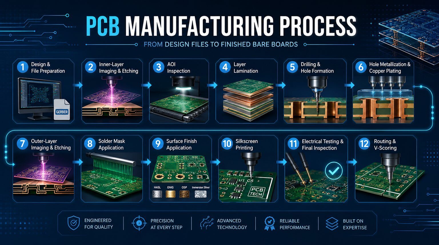
In electronics manufacturing, the PCB (printed circuit board) is the foundation of nearly every electronic device. Its quality has a direct impact on the stability and reliability of the final product. Even small defects—such as trace damage, weak solder joints, or incorrect component placement—can lead to functional problems and, in some cases, safety risks.
In the past, PCB inspection depended heavily on manual visual checks. Inspectors examined boards point by point with magnification, a method that was not only slow but also affected by fatigue and subjective judgment. As PCBs continue to move toward higher density, smaller sizes, and greater complexity, this approach is no longer enough for modern manufacturing.
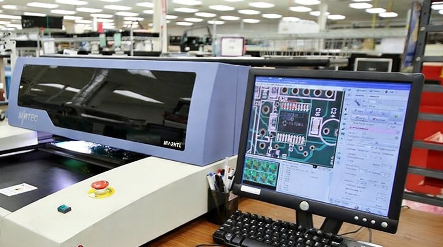
The introduction of AOI changed that. By combining high-speed imaging with intelligent inspection algorithms, AOI systems can detect solder joint issues, component placement errors, and other visible defects quickly and consistently. In real production environments, including standardized manufacturing lines such as those at PCBCool, AOI has become an important part of quality control. It helps identify potential issues after etching and reflow soldering while providing valuable feedback for process improvement.
In this article, we take a closer look at what AOI is, how it works, where it is used, and why it has become an essential part of modern PCB fabrication and assembly.
AOI stands for Automated Optical Inspection. It is an inspection method based on optical imaging and digital image processing, used to detect visible defects during PCB fabrication and assembly.
In simple terms, an AOI machine scans the surface of a PCB, captures images, and compares those images against defined standards. It then flags potential defects and marks their locations for review or repair.
The value of AOI goes beyond replacing manual visual inspection. Its real advantage is that it improves inspection speed, supports more consistent quality control, and helps manufacturers catch issues earlier in volume production.
AOI equipment uses industrial cameras and lighting systems to scan the PCB.
As the board enters the inspection area, the system applies different lighting angles and illumination methods to capture images of traces, solder joints, and component surfaces. Depending on the machine, the system may generate 2D or 3D image data.
The goal at this stage is to produce a clear visual representation of the board so the system has enough detail for analysis.
The raw image is not used as-is.
Before inspection begins, the system usually performs image preprocessing to improve contrast, reduce noise, and highlight critical edges or features.
Once the images are processed, the system can more effectively distinguish trace shapes, solder joint outlines, and component positions.
This is the core of AOI inspection.
The system compares the captured image against predefined standards, reference models, or inspection rules and looks for deviations outside acceptable limits.
Different AOI systems use different inspection methods, but common approaches include:
- Template comparison
- Feature recognition
- Edge analysis
- Grayscale or color model evaluation
- Height-based inspection in 3D AOI systems
If the system finds abnormal component placement, solder joint irregularities, incomplete traces, or other visible defects, it flags them as suspected defects.
Once inspection is complete, the AOI system outputs the defect type, location, and related image data.
Operators can then review the result and decide whether repair, rework, or further confirmation is needed.
The system can also store inspection images, defect records, and batch-level data for traceability, quality analysis, and future process improvement.
AOI and AXI are often confused in electronics manufacturing because both are automated inspection technologies used for quality control.
AOI relies on optical imaging, so it is best suited for detecting visible surface-level defects, such as:
- Component misalignment
- Missing or wrong parts
- Solder bridging
- Insufficient or excessive solder
- Opens, shorts, nicks, and other visible trace issues
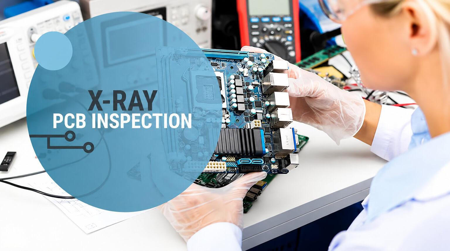
AXI, or Automated X-ray Inspection, is used for defects that cannot be seen easily through optical methods alone. It is more suitable for identifying internal or hidden issues, such as:
- Solder joint defects under BGA or QFN packages
- Voids in hidden solder joints
- Internal connection issues in multilayer structures
For that reason, AOI and AXI are not competing options. In many applications, they complement each other depending on the package type, board structure, and inspection objective.
In bare board manufacturing, AOI is often used after inner or outer layer trace formation.
At this stage, the focus is on checking the integrity and consistency of copper traces and identifying common issues such as:
- Opens
- Shorts
- Nicks
- Residual copper
- Trace width abnormalities
- Over-etching or under-etching related issues
For high-density PCB designs, this step is especially important for yield control later in production.
In SMT assembly, solder paste printing quality has a direct impact on downstream placement and soldering results.
A standard line will typically rely on SPI for paste volume and height measurement, but in some setups AOI can also serve as a supplemental method for basic visual inspection of solder paste deposits.
At this stage, the focus is usually on:
- Missing paste
- Offset printing
- Überbrückung
- Abnormal print shape
Catching these issues early helps reduce downstream defects during placement and reflow.
Post-reflow AOI is one of the most important quality control points in PCBA production.
Its main job is to verify solder quality and assembly integrity. Typical inspection items include:
- Cold or insufficient solder joints
- Too much solder
- Überbrückung
- Solder balls
- Missing components
- Wrong components
- Misalignment
- Polarity errors
- Lead-related abnormalities
The result of this inspection often has a direct impact on rework efficiency, final product reliability, and shipment risk control.
- Higher Inspection Efficiency
Compared with manual inspection, AOI is far better suited to continuous, high-volume production. It can scan large areas quickly while maintaining a stable inspection pace across batches.
- Better Inspection Consistency
Manual inspection can vary significantly depending on the operator’s experience, condition, and attention level. AOI helps reduce that variation by applying the same inspection logic across boards and batches.
- Earlier Detection of Process Issues
AOI is not only about catching bad boards. It also helps reveal process problems earlier. If a certain type of defect starts appearing repeatedly, the production team can trace it back to the relevant process step and make corrections before the issue grows into a larger yield problem.
AOI systems typically store inspection images, defect categories, and batch-related data. That information is valuable for analyzing defect patterns, identifying high-risk process steps, and supporting ongoing process optimization.
- Limited Visibility in Hidden Areas
AOI is still an optical method. If a defect is hidden under a component, inside a shielded area, or beneath a package where the camera cannot see it, AOI may not be able to detect it effectively.
- Sensitivity to Reflection and Color Contrast
On dark boards, highly reflective surfaces, or low-contrast areas, AOI can generate false calls or make detection more difficult. That is why lighting setup, program tuning, and inspection parameter optimization matter so much.
- Dependence on Program Quality
The effectiveness of AOI depends not only on the machine itself, but also on how well the inspection program is built and maintained. If the rules are too strict, false alarms can increase. If they are too loose, real defects may be missed. Stable AOI performance depends on ongoing optimization and practical production experience.
At the sample stage, some issues can still be addressed through manual review and engineering attention.
Once a project moves into volume production, however, the number of boards, the production pace, and the delivery pressure all increase. At that point, quality control is no longer just about finding defects—it becomes about finding them early, identifying them consistently, and preventing them from becoming batch-level problems.
In high-volume programs, AOI delivers value in three major ways:
- It helps catch common defects earlier in the process
- It improves inspection consistency from batch to batch
- It provides timely data for process optimization and traceability
For projects that require stable yields, controlled rework rates, and consistent delivery quality, AOI is no longer just an optional add-on. It is a key part of the quality system.
Traditional AOI systems depend heavily on rules, templates, and preset logic.
That approach works well in standardized applications, but it can require more tuning and operator intervention when dealing with complex designs, mixed product types, or borderline defect cases.
With AI increasingly being introduced into inspection systems, AOI is gradually gaining stronger sample-based learning and model optimization capability. This helps reduce false calls, improve performance in complex inspection scenarios, and make the system more adaptable across different product types and process conditions.
Traditional 2D AOI is based mainly on flat image analysis, which limits its ability to evaluate height-related issues such as lifted components, coplanarity problems, or certain solder joint shape defects.
3D AOI uses optical measurement methods such as structured light or multi-angle imaging to capture more height-related information. That makes it better suited for evaluating solder joint geometry, component height differences, and complex package structures. As a result, 3D AOI is becoming increasingly common in high-density and high-reliability applications.
In the future, AOI will not be viewed only as an inspection tool. It is increasingly becoming a critical data point within the larger manufacturing system.
When AOI data is integrated with MES, ERP, or quality management systems, manufacturers can more effectively analyze defect trends, trace batch issues, and feed inspection results back into process optimization.
That means AOI is evolving from a standalone quality checkpoint into a more connected process management tool.
The move from manual visual inspection to Automated Optical Inspection is not simply about making inspection faster.
More importantly, it makes quality control in PCB fabrication and assembly more consistent, more traceable, and more compatible with the demands of modern electronics manufacturing.
For PCB manufacturers, the maturity of their AOI capability often reflects the maturity of their overall quality control system.
Bei PCBCool, we continue to improve both our manufacturing processes and inspection capabilities in parallel. By applying AOI at key quality control points and combining it with practical PCB fabrication and assembly experience, we help customers build a more stable and controlled path from pilot runs to volume production.