Electronics in the modern world are based on the Printed Circuit Boards (PCBs). They offer a hard base, which provides mechanical support for parts and an electrical connection between them through copper traces etched on the board. The absence of PCBs would have caused electronic equipment to use loose wires, thus making them cumbersome, unreliable, and hard to fix.
In the case of students and novices, PCB design is a necessary step in transitioning between theory on circuit diagrams and the practical world. The practical skills learned through the understanding of how to transform a schematic into a real-world board include layout planning, signal routing, and signal electrical noise management.
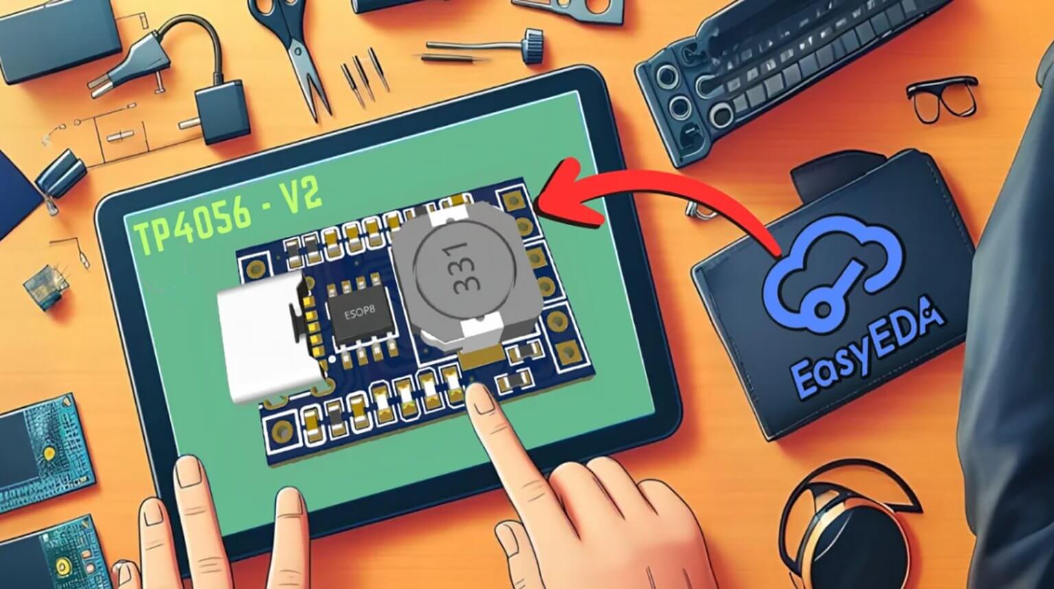
EasyEDA is online and free to use, compared to other traditional EDA software, which needs a complicated installation and high-powered hardware. It has a unified environment with schematic capture and PCB layout, simulation, and manufacturing output. This can be seen as a perfect place for a beginner to start who wishes to create a professional multi-layer PCB without any complexities of setting up the system.
The first thing to do is to create a free account on the EasyEDA site. Once you have logged in, choose the Pro Editor that offers better performance and recent editing capabilities, and supports multi-layer PCB designs.
After entering the editor, take time to familiarize the workspace. Components, libraries, and placement tools are found on the left panel. On the right panel, there are property and layer controls. The upper toolbar gives access to saving, conversion of schematics into PCBs, rule checks, and exporting manufacturing files. The central workspace is the main area where you construct your schematic and layout.
Open a new project and give it a definite name, e.g., Multilayer Controller Board. EasyEDA keeps the project on the cloud and makes it accessible on other devices, as well as safeguards your work against unintentional loss of data.
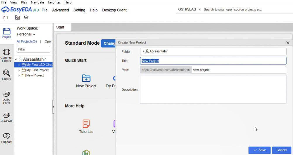
To create a new project in EasyEDA, the steps mentioned below must be followed:
- Open EasyEDA. On the top right side, there is an option for File.
- Click on File > New > Project.
- A dialog box appears, where you can give a name to your project and save it.
- After saving the project, you can see a blank schematic sheet, where you can start circuit designing.
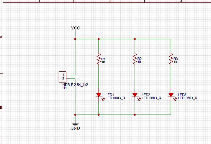
The schematic circuit is the electronic circuit blueprint. It is a representation of the electric connections of the components, but not their physical positions on the board.
Open a new sheet of schematic first and add components from the library of EasyEDA. A basic circuit based on a microcontroller, a voltage regulator, LEDs, and connectors can be used as an example of a circuit to study by a novice.
Connect the pins of the components with the wire tool in the way you want to form your circuit. Such relationships are electrical continuity. In order to maintain the schematic organized, VCC, GND, and SIGNAL net labels should be used as opposed to making long wires across the page.
Assign component values, e.g., capacitor capacitance or resistor resistance. Next, mark up the schematic in such a way that an identifier is given to every component (R1, C1, U1). This is necessary in the process of troubleshooting.
To design a circuit in EasyEDA, mentioned below steps must be followed:
- On the left side, there is an option of Library.
- Click on the library, and search for the component you want to use in your circuit.
- Connect the component pins using the wire tool.
Before the next step, the Electrical Rule Check (ERC) shall be run. This tool detects broken links, short circuits, or unpowered pins. By fixing them at this stage, you are going to be certain that you will have a working circuit when assembled.
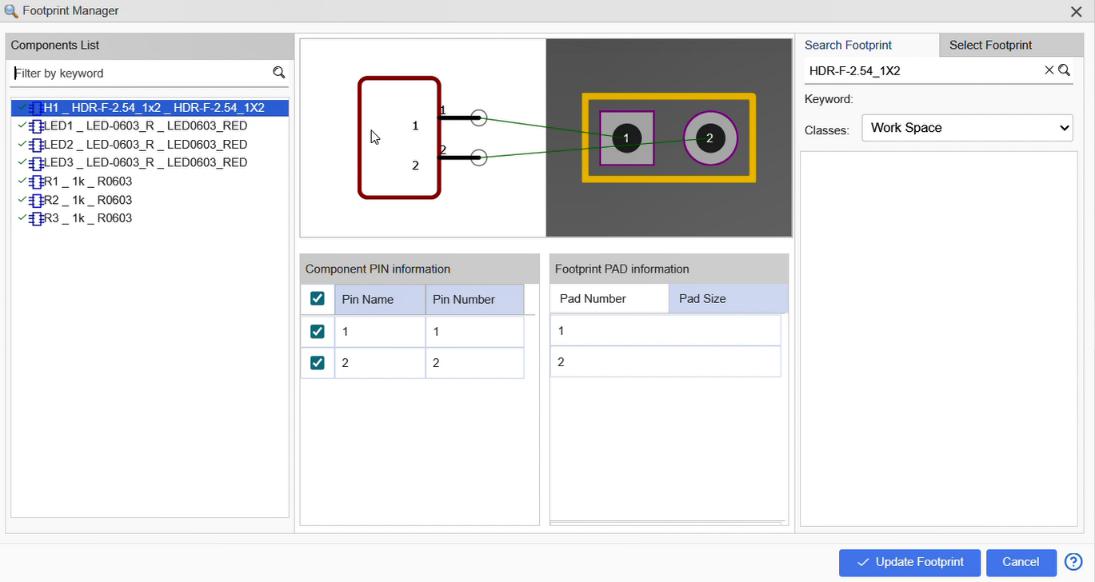
Having done the schematic, transform it into a PCB layout. The software EasyEDA provides the names of footprints assigned to each component automatically. Footprint is the arrangement and size of the physical pads of the component package.
Footprint can be assigned as follows:
- On the top menu, there is an option of tool.
- Click on Tool > Footprint Manager.
- Select the footprint and click OK. Footprint will be assigned to that component.
Footprints should be determined. Compare data sheets of components to be used in checking pad space and package type. To use a voltage regulator as an example, it can be available in various packages, and if the incorrect footprint is chosen, it will make it impossible to solder.
The beginners must use reliable library footprints so as to avoid manufacturing problems. Upon its verification, the PCB editor will open, which contains components to place.
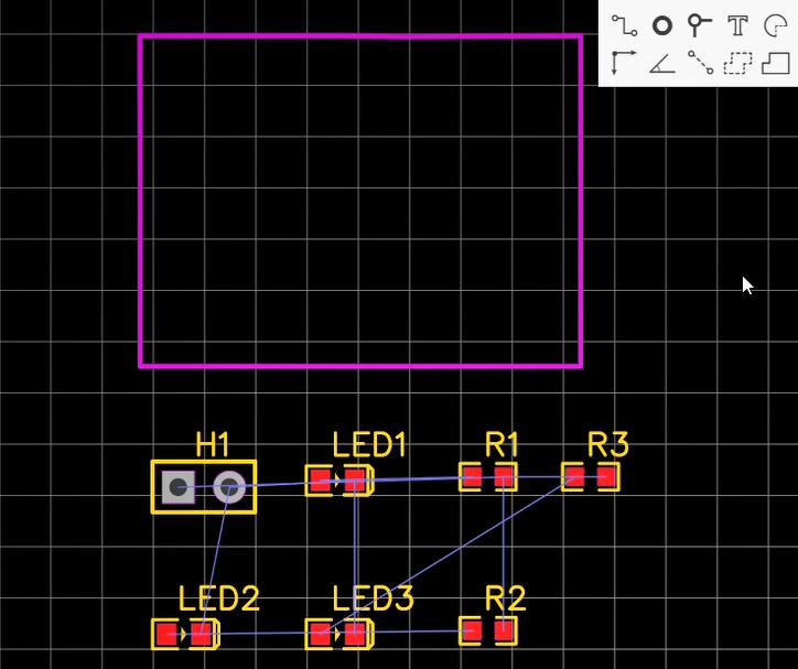
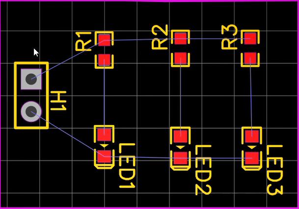
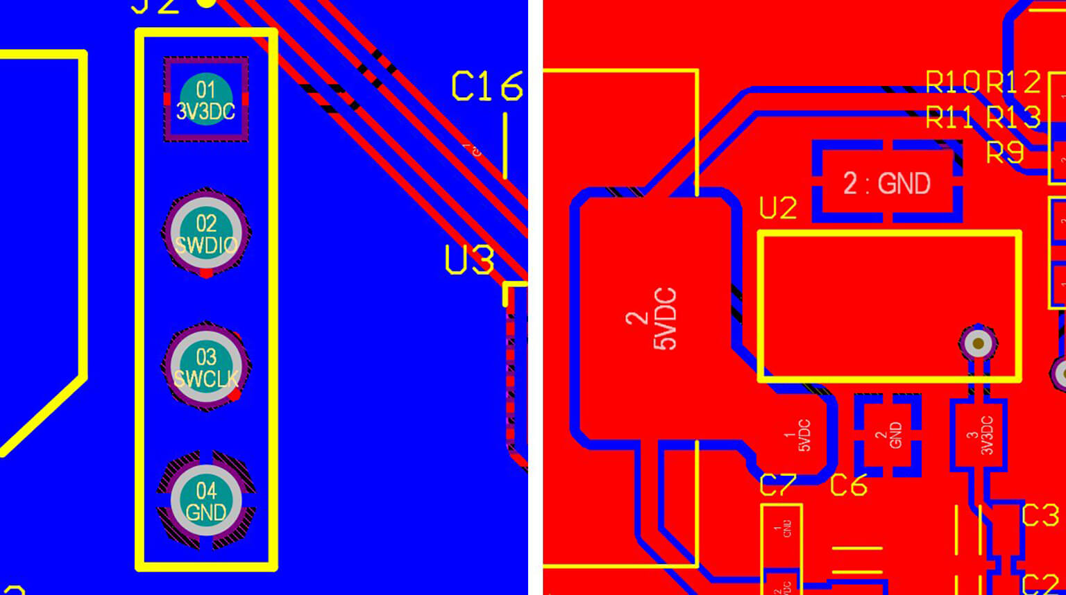
Components in the PCB editor seem to be clustered and united by fine lines known as ratsnest lines. These lines signify the work of electrical requirements.
Start by illustrating the board outline. The outline gives the physical dimension and layout of the PCB. In the case of beginners, it is simpler to work with a rectangular board. If the PCB is to be housed in an enclosure, make sure that the PCB dimensions match the requirements of the enclosure.
The board outline can be drawn as follows:
- Select the Board Outline Layer.
- On the top menu, there is an option for tools. Click Tools > Set Board Outline.
- Draw the board outline as per the requirement, and place components inside the board outline.
The second step is the logical arrangement of the components. Connectors are to be placed in the proximity of the edges of the boards. The integrated circuits should be placed centrally to reduce the trace length. The power components should be grouped together in order to make routing easy.
Proper placement is among the most critical processes in the PCB design since it determines how routing is done, electrical performance, and heat management.
In order to design a multi-layer PCB, open the settings of the layer configuration and add more copper layers. Novices in professional design techniques should use four-layers board.
There is also a general stack arrangement which consists of:
- Top layer for signal routing
- Inner Ground layer
- Power Distribution inner layer
- Bottom layer for signal routing
Ground and power planes enhance the stability of the voltage and minimize the electrical noise. They also make routing simple because of the continuous return paths of signals.
Multi-layer boards enable transfer of signals between layers through Via’s, make complex routing easier, and are capable of performance enhancement. Also, knowledge of the stacking of layers allows beginners to design complex circuits that can be applied in real-world applications.
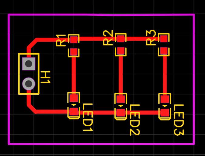
Routing is the process of connecting component pads using copper traces. Before routing the PCB, the first step is to place components. A proper placement can make routing easier and reduce the chances of error. Once the components are placed, choose the routing tool and start tracing the thin lines that represent the connection of the components.
Routing can be done as follows:
- On the top menu, there is an option for Route.
- Click on Route or use the shortcut key W for routing.
- You can also use Auto Router. Set rules before routing, click on Auto Router, and EasyEDA will route the PCB automatically.
Make traces short and straight to minimize resistance as well as signal distortion. Smooth angled turns should be used instead of sharp corners to guarantee manufacturability. Trace size depends on the functionality and the current requirement of the PCB. For Power and Ground connections, use wider traces.
In multi-layer board routing, one must use Via’s to transfer connections between layers. Via’s can be used to shift the signal from one layer to another, making complex routing easier without overlapping of traces.
Add ground planes to your PCB. Ground planes are basically copper pours that provide a continuous signal with a return path. Add copper pour and connect them to ground to enhance noise shielding and heat dissipation. A ground plane can reduce noise, increase signal integrity, and also increase signal strength.
Before completion of the design, design rules should be configured as per the manufacturer’s specifications. In design rules, we can set minimum and maximum clearance, width of traces, via diameter, and hole size, etc.
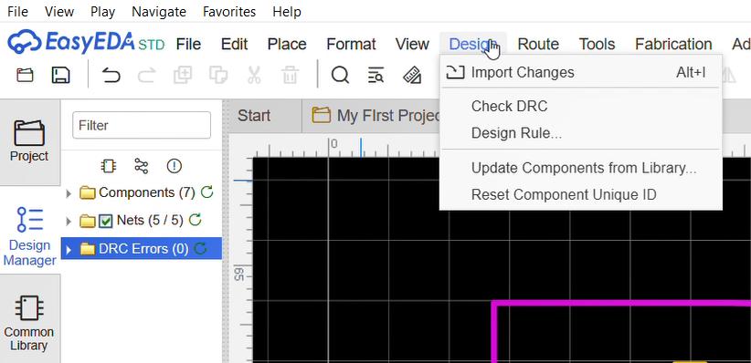
Once the PCB is completed, run the Design Rule Check (DRC). DRC will display all the errors and warnings, such as unconnected nets, short circuits, and clearance issues. Fix all the errors and warnings and run DRC again.
DRC can be run as follows:
- On the top menu, there is an option for Design.
- Click on Design > Check DRC.
To guarantee the manufacturability and avoid expensive fabrication errors, always ensure compliance with design rules.
Every component in the PCB must have a designator, and some components also have polarity. This text is known as silkscreen. Silkscreen markings provide significant information for assembly and maintenance. Add component labels and polarity, connector names, and a description of the board.
Add mounting holes in the board, which will be useful when fitting the board in an enclosure or assembly. To make debugging and measurement easier, test points may also be added.
Make sure that silkscreen text does not touch pads and copper traces, as both may create production problems.
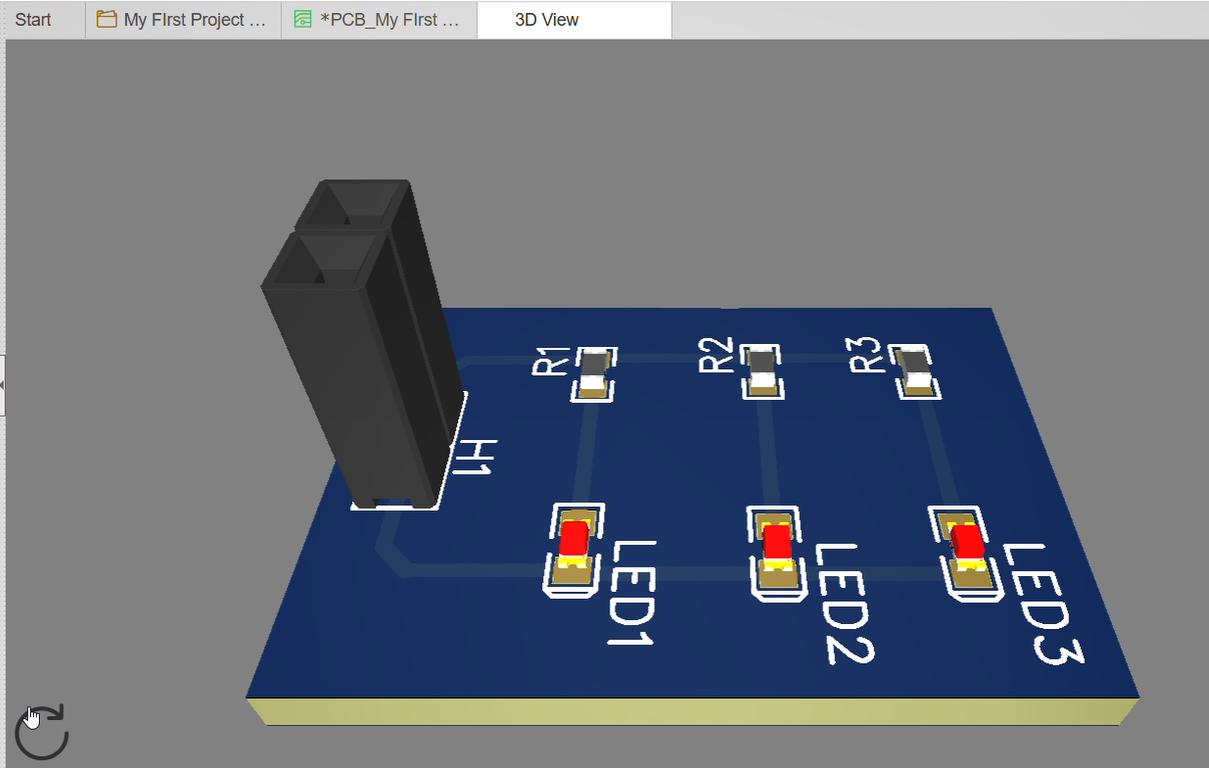
You can inspect your PCB with the help of a 3D preview before fabrication. This can be used to check the component orientation, space, and mechanical fit.
3D view of the PCB can be reviewed as follows:
- On the top menu, there is an option for View.
- Click on View > 3D Preview.
Now the next step is to produce Gerber files, which are the files that consist of all the information needed for PCB manufacturing. This is made easier by EasyEDA, and they even offer direct PCB fabrication services.
Export Bill of Materials and pick and place files in case assembly is to be automated. Once the circuit has been fabricated, the solder elements should be attached, and the circuit should be tested to verify that it is functioning properly.
Although the design of a multi-layer PCB might seem complicated at first, it becomes much more manageable with a well-structured workflow. In this tutorial, we’ve covered the complete process—from schematic creation and footprint verification to component placement, layer stack planning, routing, design rule checking, and manufacturing preparation.
PCB design is a skill that improves with practice. It’s best to start with simple circuits and gradually progress to more complex systems. Over time, you’ll develop an intuitive understanding of placement strategies, routing efficiency, and key electrical performance considerations.
Bei PCBCool, we support both beginners and professional engineers with high-quality PCB fabrication and assembly services. Whether you’re prototyping your first design or preparing for volume production, our team ensures precise manufacturing, fast delivery, and consistent results.
Start designing with EasyEDA today, and let PCBCool help you turn your ideas into real, functional hardware.