Printed Circuit Board (PCB) design goes far beyond drawing connections between components. A well-designed PCB must perform consistently throughout its entire lifecycle—from fabrication and assembly to soldering, rework, and long-term operation in real-world conditions.
Electrical correctness alone does not guarantee a successful design. In practice, one of the most common—and often overlooked—causes of manufacturing failure is poor solderability due to uncontrolled heat flow. Many boards pass schematic checks and design rule checks (DRC), yet still fail during assembly because heat does not behave the same way as electrical signals. Large copper areas, in particular, can draw heat away from pads, making proper soldering difficult.
This is exactly where thermal relief comes in. In this guide, we’ll walk through thermal relief step by step, covering both the theory behind it and how to apply it in real designs. By the end, you’ll understand not just how to use thermal relief, but why it matters, when to use it, and when it’s better to avoid it.
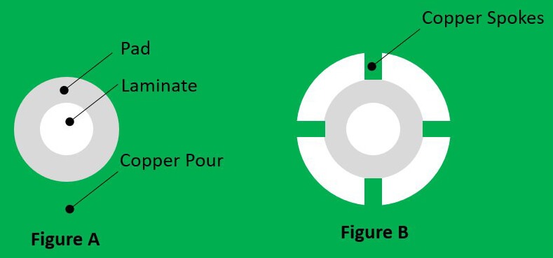
Thermal relief is a design technique used to connect a pad or via to a large copper area—typically a ground or power plane—in a controlled way. Instead of using a solid, full-width copper connection, the pad is linked to the plane through narrow copper spokes. This structure limits heat flow while still maintaining reliable electrical connectivity.
In simple terms, a solid connection allows maximum heat transfer, while a thermal relief connection intentionally restricts it.
The need for thermal relief becomes clear during the soldering process:
When heat is applied to a pad, it must quickly reach the solder’s melting temperature. However, if the pad is directly connected to a large copper plane, that plane acts as a heat sink, rapidly drawing heat away from the pad.
As a result, the pad may never reach a sufficient temperature for proper soldering. This can lead to incomplete solder melting, poor wetting, and ultimately cold solder joints. In manual soldering, this often makes the process difficult or even impossible.
Thermal relief solves this problem by increasing the thermal resistance between the pad and the surrounding copper plane. By limiting how quickly heat is dissipated, it allows the pad to heat up more efficiently and ensures more consistent soldering results.
At the center is the pad itself, which serves as the actual soldering interface. This can be a through-hole pad for component leads, an SMD pad, or in some cases a via-in-pad structure (when the process allows it).
The pad size must match the component geometry and comply with IPC soldering guidelines to ensure reliable joints.
Connecting the pad to the surrounding copper plane are the thermal spokes. These are narrow copper traces that provide both electrical continuity and controlled thermal isolation.
In most designs, spokes are evenly distributed around the pad, typically using two to four connections. Their width commonly falls in the range of 8–20 mil (0.2–0.5 mm), depending on factors such as current requirements, copper thickness, and manufacturing constraints.
By reducing the cross-sectional area of copper, the spokes limit heat flow while still maintaining a low-resistance electrical path.
Surrounding the pad and spokes is the clearance area—often referred to as the thermal relief clearance or isolation gap. This is the space that separates the pad from the solid copper plane. Its primary role is to prevent direct copper contact and control how much heat can be conducted away from the pad.
If this clearance is too small, the thermal relief becomes ineffective because heat can still flow freely into the plane. On the other hand, if the clearance is too large, the mechanical strength of the pad connection may be reduced, potentially affecting reliability under stress or during rework.
The most common configuration is the four-spoke, or crosshair, pattern. This is widely considered the industry standard because it provides a symmetrical connection between the pad and the copper plane.
The even distribution of spokes helps ensure uniform heat flow during soldering, leading to more predictable and consistent results. At the same time, the multiple connection points provide good mechanical stability, making this pattern suitable for ground pins, power pins, and through-hole connectors.
In more space-constrained layouts, a three-spoke pattern may be used. By removing one spoke, designers can save routing space or accommodate nearby features.
Although this introduces slightly uneven heat distribution, the impact is usually acceptable for most applications, especially when soldering conditions are well controlled.
A two-spoke pattern further increases thermal isolation by minimizing the copper connection to the plane. This can be helpful in situations where soldering is particularly challenging, such as with large copper pours or heavy ground planes.
However, because it reduces both thermal and electrical conduction, it is generally recommended only for low-current connections or special cases where improved solderability is critical.
In advanced designs, modified or curved spoke geometries may also be used. These variations are often found in high-density layouts, high-current planes, or controlled impedance designs, where standard straight spokes may not meet spacing or performance requirements. Such patterns are typically defined by specific design rules or CAD tool configurations rather than applied manually.
- Pads connected to large copper areas
- Hand-soldered through-hole components
- Boards that may require rework or repair
- Assemblies using wave soldering
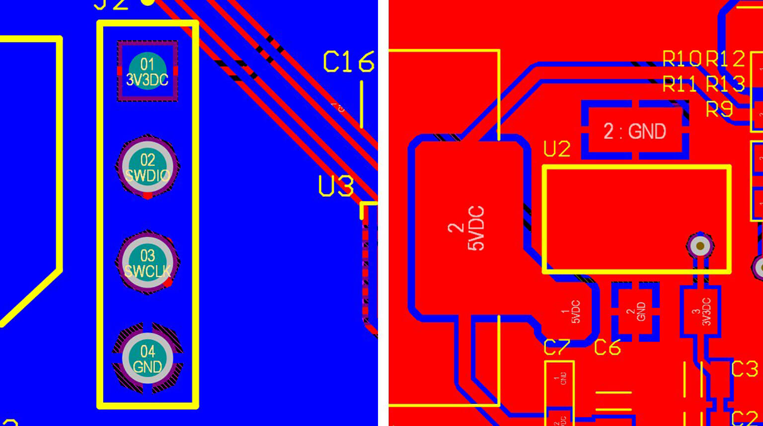
Typical use cases include ground pins of connectors, through-hole electrolytic capacitors, and test points tied to ground, where solderability is more critical than maximum current-carrying capacity.
- High-current paths where spoke capacity may be exceeded
- Applications where heat dissipation during operation is critical
- RF or high-frequency circuits requiring controlled impedance
- Pads that are part of a heat-spreading structure
Typical examples include the drain pad of a power MOSFET and the exposed ground paddle of a switching regulator, where solid connections are preferred to maximize heat transfer and electrical performance.
In most modern PCB design tools, thermal relief is applied automatically based on predefined design rules. Internally, the logic follows a pattern similar to this:
Understanding this underlying logic is important because designers frequently adjust or disable thermal relief for high-current or RF nets to ensure optimal electrical and thermal performance.
Designing thermal relief does not need to be complicated. As discussed earlier, simply connecting the pad or pin to the surrounding copper plane using spoke-like connections from four sides is usually sufficient—provided that the design adheres to the specific electrical and manufacturing requirements.
Here are typical design parameters commonly used in PCB layouts:
Spoke Width
- 10–12 mil (0.25–0.3 mm) for signal ground
- 15–20 mil (0.38–0.5 mm) for power pads
Rule of thumb: wider spokes improve current-carrying capacity but may reduce solderability.
Number of Spokes
- 4 spokes: default and most common
- 3 spokes: used in compact layouts with limited space
- 2 spokes: reserved for extreme cases where maximum thermal isolation is required
Isolation Gap (Clearance)
- Typically 6–10 mil (0.15–0.25 mm)
Always verify with your PCB manufacturer, as allowable values can vary depending on fabrication capabilities.
Thermal relief is one of those PCB design principles that may seem minor while looking at a screen, yet it becomes critically important the moment a board reaches the soldering bench. Many designers only fully appreciate its significance after experiencing the frustrating reality: a board that is electrically correct, visually clean, and fully routed still refuses to solder properly. At that point, thermal relief stops being an abstract design option and becomes a practical necessity.
Experienced PCB designers naturally consider three interconnected dimensions:
- Electrical behavior: Determines signal integrity, current flow, and functional correctness
- Thermal behavior: Governs how heat moves during soldering, operation, and rework
- Manufacturing Reality: Includes assembly methods, operator limitations, process tolerances, and yield
Bei PCBCool, we understand the critical role thermal relief plays in real-world PCB performance. Our team can assist not only with proper thermal relief design but also with the complete PCB process—from prototyping and fabrication to assembly and testing.