Designing a Printed Circuit Board (PCB) is a fundamental skill for students, electronics hobbyists, and early-career engineers who want to turn circuit concepts into real, working hardware. A well-designed PCB doesn’t just “hold components” — it directly impacts reliability, signal integrity, noise performance, and how easily the product can be manufactured.
In both academic and professional settings, OrCAD is a widely used Electronic Design Automation (EDA) tool for schematic capture, simulation, and PCB design. When paired with Cadence Allegro PCB Editor, it provides a powerful, industry-grade environment for developing complex, multi-layer boards.
This tutorial walks beginners through the complete PCB design workflow using OrCAD. Rather than just listing steps, it explains the reasoning behind each stage and shows how to execute it within the tool. By the end, you’ll be able to create schematics, assign footprints, design multi-layer layouts, route connections, run design checks, and generate the manufacturing files needed for fabrication.
Before getting started, it’s important to understand how OrCAD structures the PCB design process. Like most professional EDA tools, OrCAD follows a step-by-step workflow that takes your circuit from concept to a manufacturable board.
The process begins with schematic capture in OrCAD Capture, where you define the logical design of the circuit. Once the schematic is complete, each component is assigned a physical footprint that represents how it will be mounted on the PCB.
The design is then transferred to OrCAD PCB Editor (Allegro). This is where you define the board outline, place components, and route all electrical connections between them.
The final stage includes running design rule checks (DRC) to catch issues such as spacing violations or connectivity errors. After verification, you generate manufacturing outputs—typically Gerber-Dateien and drill data—which are sent to the PCB manufacturer.
Before starting any design work, you’ll need to install and properly set up the OrCAD software. Many universities provide student versions, and trial versions are also available for individual learners.
Once OrCAD is installed, it’s a good idea to create a dedicated project folder to keep all design files organized. You should also verify that your library paths are configured correctly so components and symbols can be accessed without issues.
Another key step is making sure OrCAD Capture is properly integrated with OrCAD PCB Editor (Allegro). This connection allows you to seamlessly transfer your schematic design into the PCB layout environment later in the workflow.
Spending a few minutes checking these settings upfront can save a lot of frustration down the road by preventing missing libraries, incorrect footprint assignments, and file linking errors.
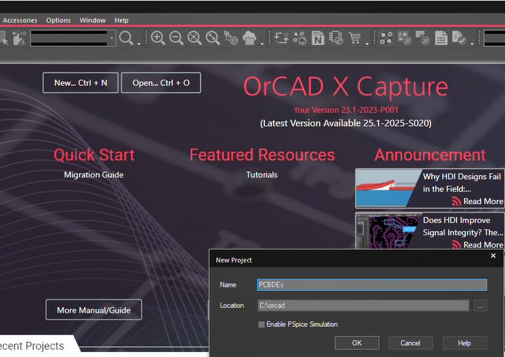
With OrCAD installed and configured, the next step is to create a new PCB project. In OrCAD Capture, go to File → New → Project, then select PCB Project. Choose a clear project name and specify a folder where all related design files will be stored.
Once the project is created, OrCAD will open a blank schematic page. This workspace is where you’ll build the logical representation of your circuit before moving on to the physical PCB layout.
To summarize, creating a new project involves:
- Navigating to File → New → Project
- Selecting PCB Project
- Entering a project name and choosing a save location
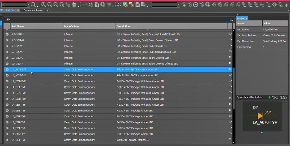
With your project set up, the next step is to place components onto the schematic. In OrCAD Capture, you can open the component selection dialog by choosing Place → Part.
If the component you need isn’t listed, you can load additional libraries by selecting Add Library and browsing to the appropriate OrCAD library files. For beginners, it’s best to start with common components such as resistors, capacitors, diodes, integrated circuits (ICs), connectors, and voltage sources.
To add components to your schematic:
- Go to Place → Part
- Search for the desired component (e.g., resistor, capacitor, IC)
- Select the component and place it on the schematic sheet
- Arrange components in a logical layout based on circuit function
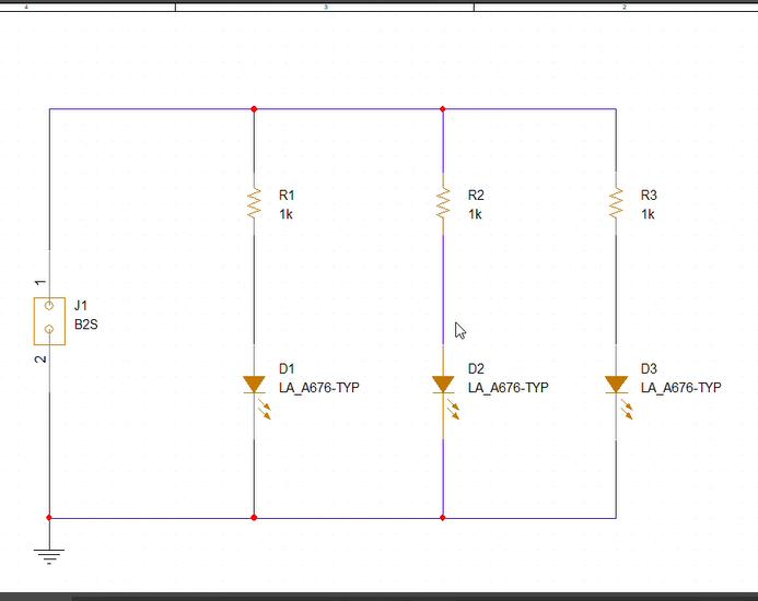
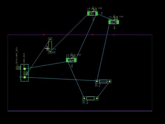
After placing components, the next step is to connect them using wires. In OrCAD Capture, you can draw connections by selecting Place → Wire or using the shortcut Shift + W.
When wiring your schematic, try to keep the layout clean and easy to follow. Avoid unnecessary wire crossings, as they can make the design harder to read and debug. For signals that span across the schematic—such as power and ground—it’s best to use net aliases. Naming signals like VCC and GND improves readability and helps ensure correct connectivity during PCB layout.
To wire your circuit:
- Go to Place → Wire (or press Shift + W)
- Click between component pins to create connections
- Use net aliases to label important signals
Once the wiring is complete, you should assign proper values and properties to each component. This ensures the design accurately reflects real-world parts and behaves correctly during simulation and layout.
To edit component properties:
- Double-click on a component
- Open the properties dialog
- Enter values such as resistance, capacitance, voltage rating, or part number
It’s also important to verify pin numbering and orientation against the component’s datasheet to avoid mismatches later in the PCB layout stage.
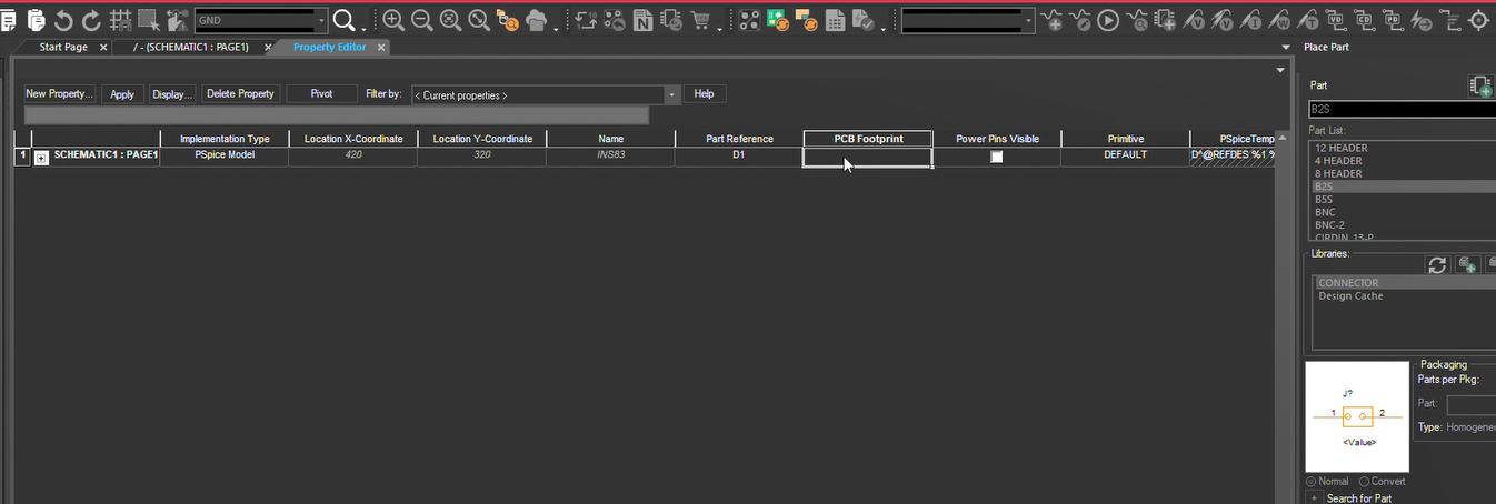
Each component in your schematic must be linked to a physical footprint that represents its real-world package on the PCB. This step is critical, as the footprint determines how the component will be placed and soldered during manufacturing.
In OrCAD, footprints are typically assigned through the component’s properties. You can either manually enter the footprint name or use built-in tools (such as the footprint assignment interface) depending on your setup.
To assign a footprint:
- Open the component’s properties (double-click the component)
- Locate the PCB Footprint field (often labeled Footprint or PCB Footprint)
- Enter or select the appropriate footprint from your library
- Apply the changes to update the component
In some workflows, you may also use OrCAD’s footprint assignment tools to batch-assign footprints across the entire design, which can be more efficient for larger projects.
Always verify the footprint against the component’s datasheet before finalizing your selection. Pay close attention to package type, pin spacing (pitch), and dimensions. Using an incorrect footprint can lead to assembly issues or even render the PCB unusable.
Once your schematic is complete and all footprints have been assigned, the next step is to move the design into the PCB layout environment.
In OrCAD Capture, this is typically done by generating the layout data (often referred to as a netlist or design transfer file) and importing it into OrCAD PCB Editor (Allegro).
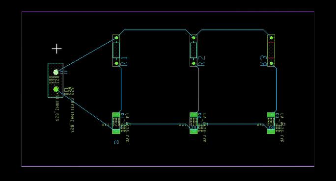
After transferring the design, open it in the PCB Editor. You’ll see a blank board outline (or workspace), with all components placed outside the board boundary. These components are now ready to be arranged and routed.
To generate and open the PCB layout:
- Go to Tools → Create Netlist (or use the PCB Editor export option)
- Launch OrCAD PCB Editor (Allegro)
- Import or open the generated design file
At this stage, the PCB layout process begins—starting with defining the board outline, followed by component placement and routing.
Before placing components, you’ll need to define the board outline. This outline determines the physical shape and size of your PCB, and it should match your mechanical and enclosure requirements. Even small mistakes at this stage can lead to fitment issues during assembly.
To define the board shape:
- Set the active class/subclass to Board Geometry → Design Outline
- Use Add → Line (or other shape tools) to draw the board perimeter
- Once the outline is complete, go to Shape → Create Shape from Lines
- Select the drawn outline and confirm to generate the board shape
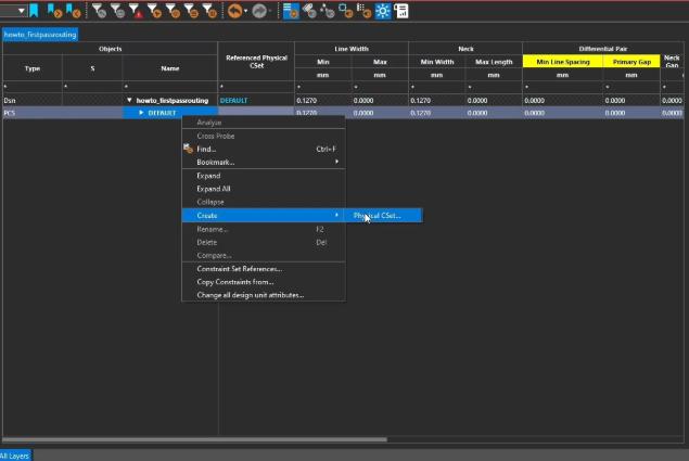
Before placing and routing components, it’s important to define your design rules. Setting these constraints early helps prevent errors, simplifies routing, and ensures your PCB meets manufacturing requirements.
In OrCAD PCB Editor (Allegro), design rules are managed through the Constraint Manager. This is where you define electrical and physical constraints for your board.
To set design rules:
- Go to Setup → Constraints (or open the Constraint Manager from the toolbar)
- Define trace widths based on current requirements
- Set spacing (clearance) constraints between traces, vias, and components
- Specify via sizes and drill diameters
- Configure additional rules as needed (e.g., differential pairs, impedance, net classes)
These constraints guide the layout process and are enforced during routing and design rule checks (DRC).
Component placement has a major impact on PCB performance, signal integrity, and ease of routing. Following good placement practices early in the layout process will make the design more reliable and easier to manufacture.
Here are some key guidelines for beginners:
- Place connectors and test points near board edges for easy access.
- Large components, such as microcontrollers or FPGAs, should generally be positioned near the center of the board.
- Position decoupling capacitors close to IC power pins to reduce noise and improve power stability.
- Keep analog and digital sections separate to minimize interference between sensitive and noisy signals.
- Group related components together to shorten trace lengths and reduce signal delays.
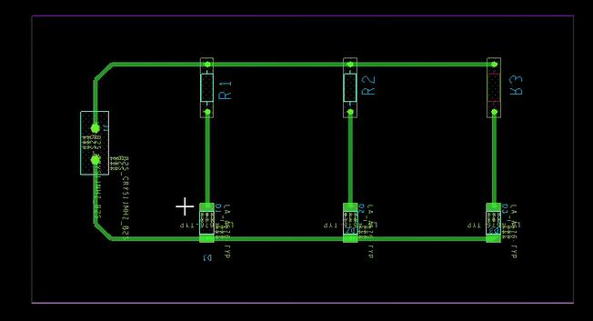
Routing is the process of connecting component pads with copper traces, turning your schematic into a functional PCB. Good routing practices are essential for signal integrity, power delivery, and overall board reliability.
Key steps:
- Go to Route in the top menu bar.
- Click on component pads to start drawing traces.
Key guidelines:
- Keep traces as short and direct as possible to reduce noise and signal delay.
- Power and ground traces should be wider to handle higher current without excessive voltage drop.
- Avoid sharp 90-degree corners; use 45-degree angles to maintain signal integrity.
- Vias can be used on multi-layer boards to switch signals between layers.
- Use a continuous ground plane where possible to minimize electromagnetic interference (EMI) and provide a low-impedance return path for signals.
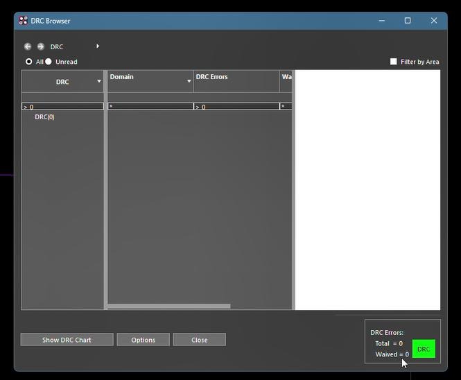
Once routing is complete, the next step is to run a Design Rule Check (DRC). This step verifies that your layout meets the constraints you defined earlier and helps catch issues before manufacturing.
DRC identifies problems such as clearance violations, unrouted nets, short circuits, and overlapping or improperly spaced traces. Addressing these issues ensures the PCB meets both electrical and manufacturing requirements.
To run a DRC in OrCAD PCB Editor (Allegro):
- Go to Tools → Design Rule Check
- Run the DRC process
- Review the generated report, which lists all errors and warnings
- Fix any issues in the layout
- Re-run DRC until no critical errors remain
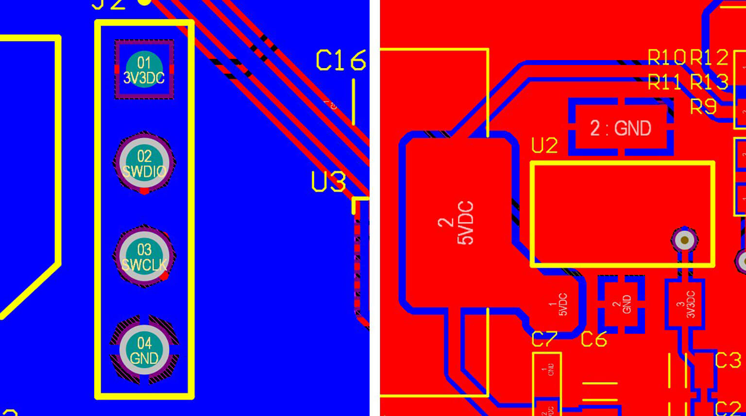
Silkscreen markings are used to label components and provide important information for assembly, testing, and maintenance. A clear and well-organized silkscreen layer makes it much easier to identify parts and reduces the risk of assembly errors.
Typical silkscreen elements include:
- Reference designators (e.g., R1, C1, U1) to identify each component
- Polarity markings for components such as diodes, electrolytic capacitors, and LEDs
- Pin 1 indicators for ICs and connectors to ensure correct orientation
- Board information, such as the board name, revision number, or company logo
Before sending your design out for fabrication, it’s essential to perform a final review. This step helps catch any remaining issues and ensures the board will function as expected once manufactured.
Key items to verify include:
- Component orientation, especially for polarized parts and ICs
- Footprint accuracy, ensuring each component matches its physical package
- Drill sizes for vias and through-hole components
- Board dimensions and overall mechanical constraints
- Connectivity, confirming there are no missing or incorrect connections
- Design Rule Check (DRC) results, ensuring no unresolved violations remain
Designing a PCB using OrCAD may seem challenging at first, especially if you’re new to the process. However, once you understand the workflow and follow a structured, step-by-step approach, it becomes much more manageable—even for beginners.
From schematic capture and footprint assignment to layout, routing, verification, and manufacturing outputs, each stage plays a critical role in creating a reliable and manufacturable PCB. Skipping or rushing any step can lead to issues later, so building a solid foundation is key.
If you’re looking to move faster or need expert support, PCBCool offers professional PCB design services and engineering guidance at every stage of development. From initial concept to final layout—and all the way through PCB fabrication and assembly—we help turn your ideas into fully functional, production-ready PCBA boards.