Although we often hear the term “microwave,” it’s not something most of us encounter in everyday electronics—and even when we do, it can be hard to recognize. Microwave technology, which deals with high-frequency electromagnetic signals, is most commonly found in applications like cellular base stations, radar systems, and advanced imaging equipment. Designing for these scenarios requires careful attention to signal loss, impedance control, electromagnetic interference (EMI), and material selection.
This tutorial aims to demystify microwave PCB design by tackling these challenges head-on. Whether you’re a hobbyist stepping into high-frequency design for the first time or a professional looking to refine your skills, this guide will give you practical insights to build more reliable and efficient microwave circuits.
Microwave Printed Circuit Boards (PCBs) are specialized boards designed to operate at very high frequencies—typically anywhere from 1 GHz to 300 GHz. At these frequencies, electrical behavior changes dramatically compared to conventional, lower-frequency circuits. In fact, many of the assumptions used in standard PCB design start to break down once you go beyond roughly 1 GHz.
At low frequencies, interconnects are electrically short compared to the signal wavelength. Designers can rely on lumped-element approximations and assume signals propagate almost instantaneously across traces. At microwave frequencies, however:
- Signal propagation delay becomes significant relative to the signal period.
- Distributed capacitance and inductance dominate circuit behavior.
- Electromagnetic fields extend beyond copper traces.
- Return current paths play a critical role in shaping impedance and radiation.
- Discontinuities in the layout cause measurable signal reflections.
The key takeaway: microwave PCB design is really about shaping electromagnetic structures, not just connecting components.
Think of a microwave PCB as a 3D medium guiding electromagnetic fields. Every trace, plane, via, dielectric interface, and enclosure becomes part of the RF system. To design effectively, engineers must consider:
- Transmission line theory
- Electromagnetic boundary conditions
- Material dispersion
- Thermal expansion
- Manufacturing tolerances
Unlike digital PCB, where timing margins can absorb minor errors, microwave systems operate with tight amplitude and phase budgets. Even small deviations in geometry can lead to problems like:
- Return loss degradation
- Gain ripple
- Group delay distortion
- Phase mismatches in array systems
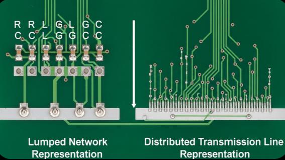
In low-frequency electronics, we often treat components as discrete resistors, inductors, and capacitors located at specific nodes. Voltage and current are assumed uniform along the conductors, making analysis straightforward.
At microwave frequencies, this assumption no longer holds:
When a trace exceeds about λ/16 in length, distributed modeling becomes mandatory.
Transmission lines are described by four distributed parameters:
- R’ – resistance per unit length
- L’ – inductance per unit length
- G’ – conductance per unit length
- C’ – capacitance per unit length
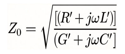
These parameters define the characteristic impedance:
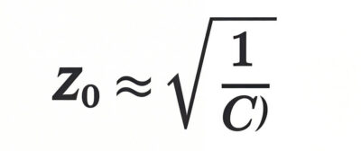
For low-loss microwave lines:
Practical implications:
A 15 mm trace at 10 GHz is not just a simple connection—it can act as:
- A resonator
- A delay element
- A phase shifter
- A source of reflection
If trace lengths are not carefully controlled, they can unintentionally filter signals or introduce reflections, degrading the performance of your circuit.
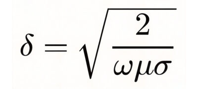
Alternating magnetic fields inside a conductor induce eddy currents that push most of the signal current toward the surface. This means that the bulk of the conductor is barely used.
Skin depth calculation formula:
For example, standard 1 oz copper is about 35 µm thick. At microwave frequencies:
- 1 GHz → δ ≈ 2 µm
- 10 GHz → δ ≈ 0.66 µm
- 60 GHz → δ ≈ 0.27 µm
As a result, over 98% of the conductor thickness is effectively unused.
Engineering consequences include:
- Surface roughness significantly increases effective resistance.
- Electrodeposited (ED) copper can introduce additional loss.
- Rolled annealed (RA) copper is preferred for mmWave designs.
- Silver plating reduces surface resistance, improving performance.
- ENIG finishes may slightly increase loss due to the nickel layer.
- EM simulations should include surface roughness correction models to predict losses accurately.
Dielectric loss occurs because dipoles in the material lag behind the rapidly alternating electric field.
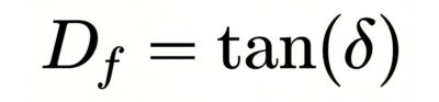
Loss tangent calculation formula:
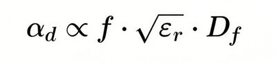
Dielectric attenuation calculation formula:
Above roughly 6–10 GHz, low-loss materials are mandatory. For reference:
| Material | Dk | Df |
|---|
| FR-4 | 4.2–4.8 | 0.015–0.025 |
| RO3003 | 3.0 | 0.0013 |
| RO4350B | 3.66 | 0.0031 |
Wichtige Überlegungen:
- Lower Df (loss tangent) is more important than lower Dk for minimizing loss.
- Stable Dk across temperature is critical for phase-sensitive designs.
- Dielectric anisotropy must be considered in multilayer PCB.
In phased arrays, even small variations in Dk can cause beam steering errors.
At mmWave frequencies, conductor surface roughness can account for up to 40% of insertion loss. Designers commonly use models like:
- Hammerstad correction factor
- Huray “snowball” model
Best practices:
- Obtain surface roughness parameters from your laminate supplier.
- Include roughness effects in 3D EM simulations.
- Compare simulated and measured insertion loss to validate your design.
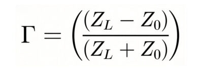
At microwave frequencies, every PCB trace acts as a transmission line. This means that the signal “sees” a characteristic impedance (Z_0), which is typically 50 Ω in RF systems. If the load impedance (Z_L) does not match Z_0 exactly, part of the signal reflects back toward the source instead of being fully delivered to the load.
The reflection coefficient (Γ) quantifies this effect:
When Z_L = Z_0, there’s no reflection. Any deviation creates reflected waves, which can lead to standing waves, gain ripple, reduced efficiency, and even instability in high-gain RF circuits.
Microwave systems are extremely sensitive to small impedance variations because the wavelength shrinks as frequency increases. Even minor changes in trace width, dielectric thickness, or copper roughness can shift impedance enough to create measurable reflections.
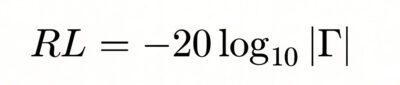
For example, in a 50 Ω system:
- 5% mismatch (≈52.5 Ω) → Return loss ≈ 26 dB (a small but measurable reflection)
- 10% mismatch (≈55 Ω) → Return loss ≈ 20 dB (significant enough to degrade performance)
Return loss (RL) is related to Γ by:
High-performance RF and microwave systems—such as radar front ends, satellite transceivers, phased arrays, and 5G modules—typically aim for >20–25 dB return loss, and sometimes >30 dB on critical paths.
Even a small drift beyond ±2% in impedance can cause:
- Increased VSWR (voltage standing wave ratio)
- Reduced amplifier efficiency
- Gain ripple across frequency
- Phase distortion
- Potential oscillation in sensitive circuits
Because of this, stack-up thickness, dielectric constant tolerance, copper etching precision, and manufacturing repeatability must be tightly controlled. In microwave PCB design, impedance control is not optional—it’s essential for predictable electromagnetic performance.
A trace requires controlled impedance if its length exceeds roughly λ/16.
Example: On a Dk = 3.5 substrate at 5 GHz:
- Wavelength λ ≈ 32 mm
- λ/16 ≈ 2 mm
This means even very short traces may need controlled impedance to avoid reflections.
Microstrip lines have their fields partly in the dielectric and partly in air. This makes them relatively easy to design and fabricate, but the effective dielectric constant depends on the field distribution:
Design considerations:
- Radiation loss increases with frequency.
- Impedance is sensitive to variations in copper thickness and trace width.
- Discontinuities at bends or vias can create reflections and must be carefully optimized.
Stripline is a trace sandwiched between two ground planes and fully enclosed in dielectric material.
Vorteile:
- Excellent isolation from external signals
- Very low radiation
- Stable and predictable impedance
Challenges:
- Harder to probe and debug signals
- Via transitions are more complex
- Slightly higher dielectric loss because the electromagnetic field is fully confined inside the substrate
Stripline is common in high-performance multilayer microwave and RF PCB where signal integrity and isolation are critical.
CPW lines have the signal trace and ground traces on the same layer, separated by a narrow gap.
Why CPW is popular:
- Easy shunt grounding: ground vias can be placed very close to the signal line
- Better integration with MMICs (monolithic microwave integrated circuits)
- Lower radiation compared to standard microstrip
Common applications:
- 24 GHz radar systems
- 60 GHz WiGig communication
- mmWave RF modules
CPW is especially useful for high-frequency and compact layouts because it improves grounding, reduces radiation, and supports integration with advanced RF components.
Capacitive coupling happens when the electric fields of adjacent traces interact. Essentially, a voltage change on one trace can induce an unwanted voltage on a neighboring trace.
Coupling becomes stronger when:
- Traces are spaced too closely
- Parallel trace lengths are long
- High dielectric constant (Dk) materials are used, which store more electric energy
Mitigation strategies:
- Maintain adequate spacing between traces
- Place ground or guard traces between sensitive lines
- Optimize the PCB stack-up to reduce overlap of high-frequency fields
Inductive coupling occurs through the magnetic fields generated by current loops in traces. When these fields link with neighboring loops, they induce unwanted currents, causing interference. The susceptibility depends largely on the loop area of signal paths.
Mitigation strategies:
- Keep return current paths tight and close to the signal traces
- Use solid ground planes to provide low-inductance return paths
- Avoid ground splits or breaks that force return currents to take longer detours
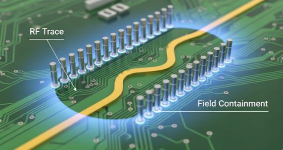
A via fence is a row of vias connecting multiple ground layers around a signal trace or cavity. It acts like a shield to confine electromagnetic fields and reduce interference.
- Spacing rule: roughly λ/20 or closer
- Purpose:
- Contain high-frequency fields
- Reduce radiation and interference
- Improve isolation between adjacent traces or circuits
Via fences are especially important in stripline and coplanar waveguide designs,
as well as for high-power microwave traces, to prevent leakage and maintain tight impedance control.
Dk is a key property to consider. It influences impedance, signal velocity, and trace width. Materials with a lower Dk allow for wider traces, which reduces conductor loss and makes fabrication easier. Higher Dk materials enable smaller, denser layouts but can increase dielectric loss.
Df determines how much signal energy is lost as heat within the substrate. For high-frequency designs:
- Around 10 GHz, use materials with Df < 0.005
- For mmWave applications, aim for Df < 0.002
Choosing low-Df materials is essential to maintain signal integrity and minimize loss.
The thermal coefficient of Dk (TCDk) describes how the dielectric constant changes with temperature. This is especially important in:
- Phased array antennas
- Frequency-stable oscillators
- Precision filters
Temperature-induced phase drift or frequency shifts can significantly impact performance. Selecting materials with low TCDk ensures signals remain stable across temperature changes, providing reliable operation.
Microwave power amplifiers generate localized heating, which affects:
- Dielectric constant (Dk)
- Conductor resistance
- Gain stability
Mitigation strategies include:
- Thermal vias
- Copper “coins”
- Aluminum-backed laminates
- Heat spreaders
- Direct-bonded copper
For RF sections above 5 W, performing thermal simulation is highly recommended to ensure safe and stable operation.
By understanding the core design principles, selecting the right low-loss materials, applying sound layout practices, and using accurate simulation and testing methods, engineers can build microwave PCB that meet the demanding requirements of modern electronic systems. As frequencies continue to rise, mastering these fundamentals becomes essential for developing reliable and high-performance designs.
At the same time, working with an experienced partner can make a significant difference. At PCBCool, we have extensive experience handling microwave PCB projects—from design support and material selection to fabrication and assembly. Whether you’re developing a prototype or scaling to production, our team is ready to help you bring your design to completion with confidence.