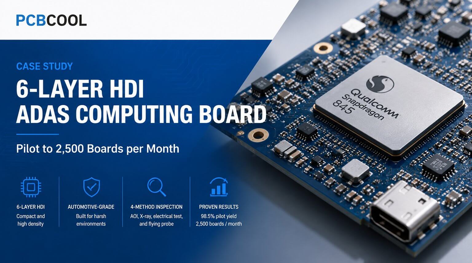
PS Electronics manufactured a 6-layer HDI board for an open-source ADAS computing device — routing a Qualcomm Snapdragon 845 BGA through laser-drilled microvias and via-in-pad structures on high-Tg FR4 with ENIG finish. The 1,000-unit pilot run achieved 98.5% yield under a four-method inspection protocol (AOI, X-ray, electrical test, flying probe), and the program has transitioned to steady monthly production of 2,500 boards.
Now, let’s look at the project and how PS Electronics helped the customer solve the manufacturing problems.
An open-source autonomous driving software company, founded in 2016 in the US. Their driver-assistance platform supports hundreds of vehicle models worldwide — pure camera-based vision, no LiDAR, no radar. The company develops both the software stack and the windshield-mounted computing hardware that runs it.
- Three automotive-grade cameras — two forward-facing (wide + narrow), one infrared driver-monitoring camera
- Qualcomm Snapdragon 845 SoC — octa-core Kryo 385 at 2.8 GHz, Adreno 630 GPU, 3rd-gen AI Engine for real-time trajectory prediction
- GPS/IMU, LTE modem, Bluetooth 5.0, USB-C expansion
- Samsung SSD (250 GB) for local data logging
The device mounts directly to the windshield. Cabin temperatures under direct sun regularly hit 85 °C and spike higher. Users in hot climates have documented thermal throttling and hardware degradation from sustained heat.
Here’s the PCB inquiry information the customer sent to us:
The Snapdragon 845 sits in a 12.4 mm × 12.4 mm Molded Embedded Package BGA. At this pitch, surface-layer dog-bone routing is geometrically impossible — not enough space between pads to escape signals using conventional plated through-holes.
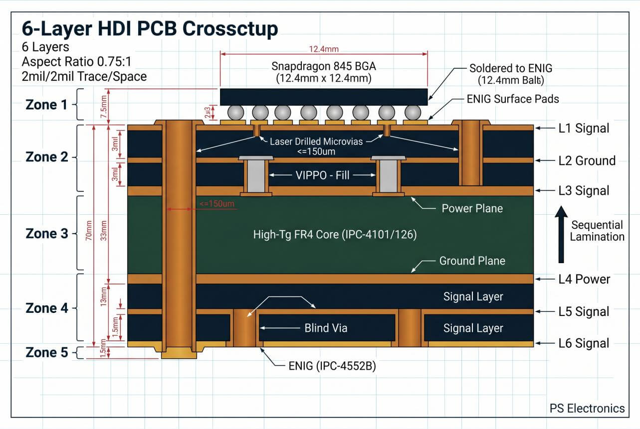
That requires a high-density build: laser-drilled microvias (≤150 μm finished hole, per IPC-2226), via-in-pad plated over (VIPPO) to drop signals directly from BGA pads to inner layers, and sequential lamination to build up microvia layers over the core.
Without UV/CO2 laser drilling, vacuum via-plugging for VIPPO, and the controlled environment sequential lamination requires — this board does not get built.
Too large for quick-turn prototype houses. Per-unit costs at prototype pricing make 2,500 units financially unviable. Prototype shops lack the volume material procurement to keep HDI laminate costs reasonable.
Too small for Tier-1 EMS attention. Major contract manufacturers optimize for runs of 50,000+. A 2,500-unit HDI program triggers MOQ penalties, gets deprioritized during peak seasons, and suffers from long lead times.
Too complex for regular PCB factories. Standard multilayer facilities do not own laser drilling or sequential lamination equipment. Sending this work to a factory without corresponding abilities may result in outsourced sub-processes, split accountability, and yield problems.
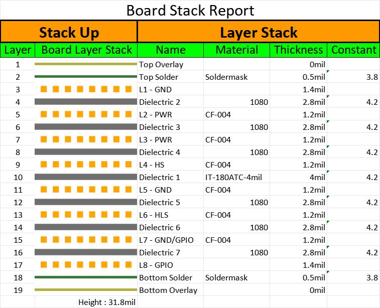
The 6-layer stackup uses high-Tg FR4 laminate (IPC-4101/126, Tg 170–200 °C) with ENIG surface finish per IPC-4552B. Microvias are laser-drilled at ≤150 μm diameter with an aspect ratio held at 0.75:1 — tighter than the IPC-2226 maximum of 1:1 — to ensure uniform copper deposition during electroplating. Via-in-pad structures let BGA signals escape directly to inner routing layers.
PS Electronics fabricates rigid PCBs from 1 to 40 layers at 2 mil/2 mil (50 μm) trace and space. The Snapdragon 845 escape routing sits within standard production capability, not at the edge of what the factory can do.
The engineering team ran a manufacturability review before quoting. The Gerber package passed clean — the client’s layout was HDI-ready from the start. DFM confirmation covered BGA pad geometry, microvia placement relative to thermal zones, copper balance across layers, and panel utilization.
The program followed a staged ramp: 1,000-unit pilot for process validation, then step pricing at 5K / 10K / 15K. A 30-person startup does not want to commit six figures of production spend before seeing yield data. This model gives them that data first.
Three material decisions matter here — each one tied to the realities of a board that lives on a car windshield.
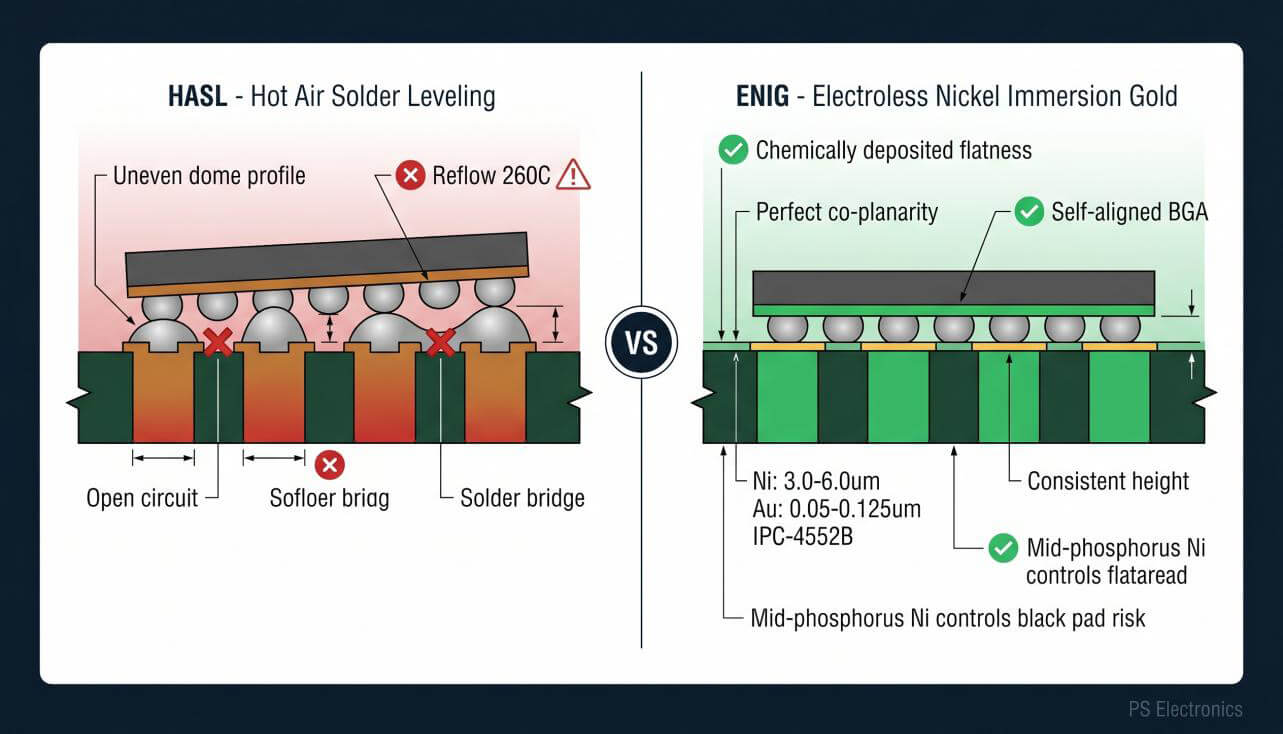
HASL leaves dome-shaped solder deposits. Put a rigid 12.4 mm BGA over uneven HASL pads and you get open circuits and bridging during reflow. ENIG gives you chemically deposited flatness.
But ENIG has its own failure mode: black pad syndrome. Aggressive gold bath chemistry hyper-corrodes the nickel barrier, leaving a brittle phosphorus-rich layer underneath that fractures invisibly under thermal cycling. IPC-4552B controls this — nickel at 3.0–6.0 μm, gold at 0.05–0.125 μm, mid-phosphorus content tightly managed.
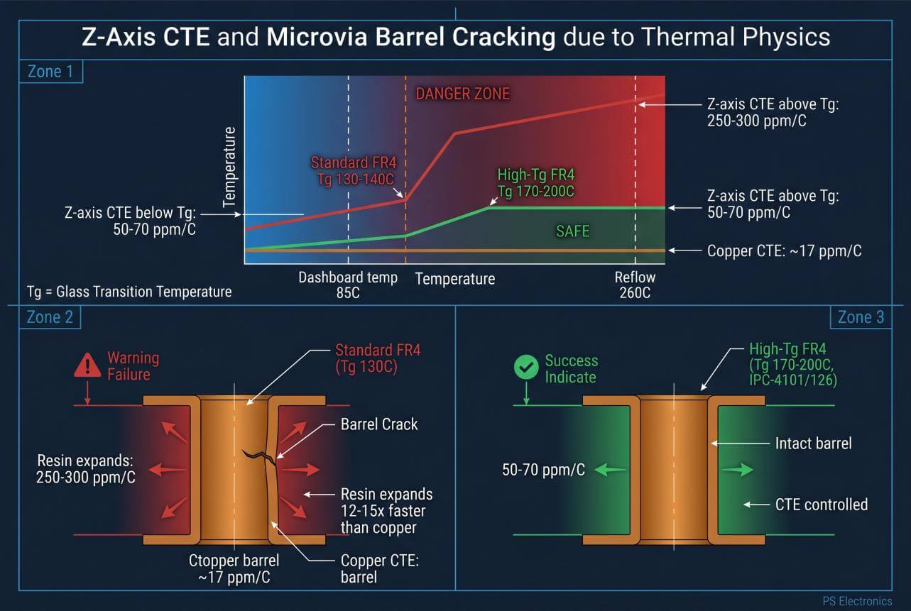
Here is the physics. Below Tg, FR4 has a Z-axis CTE of 50–70 ppm/°C. Above Tg, that number jumps to 250–300 ppm/°C. Copper via barrels expand at ~17 ppm/°C.
So when a standard FR4 board (Tg 130–140 °C) hits 260 °C during lead-free reflow — or sits at 85 °C+ on a Texas dashboard for years — the resin expands vertically 12–15x faster than the copper barrel. The barrel cracks. High-Tg laminate (Tg 170–200 °C, per IPC-4101/126) pushes that failure threshold well above operating and reflow temperatures.
The Snapdragon 845 BGA packs hundreds of pins into a 12.4 mm × 12.4 mm footprint. VIPPO places microvias directly inside the BGA pads — filled with epoxy, planarized, plated over. Signals drop to inner layers immediately, bypassing the surface congestion that would otherwise force the design into 8+ layers or a bigger board.
The first stage was a 1,000-unit pilot:
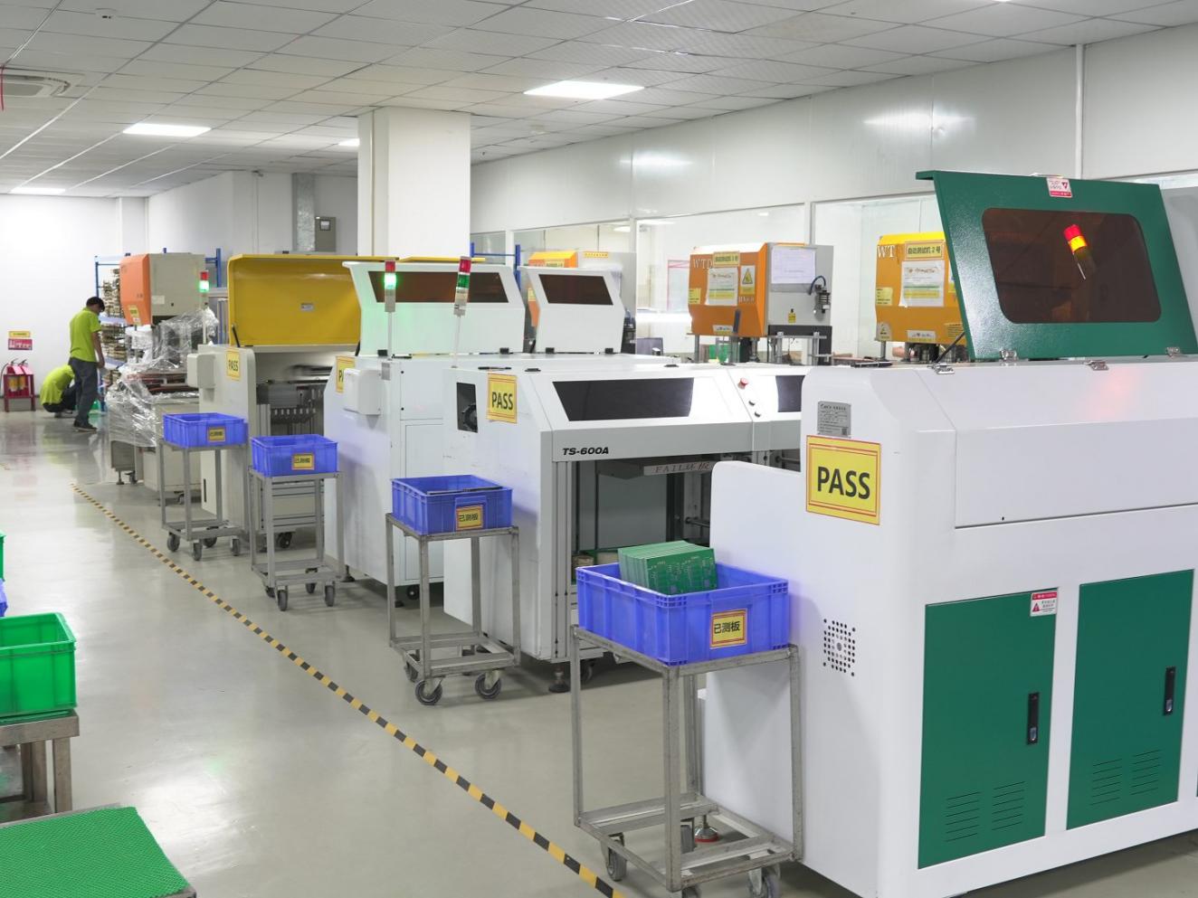
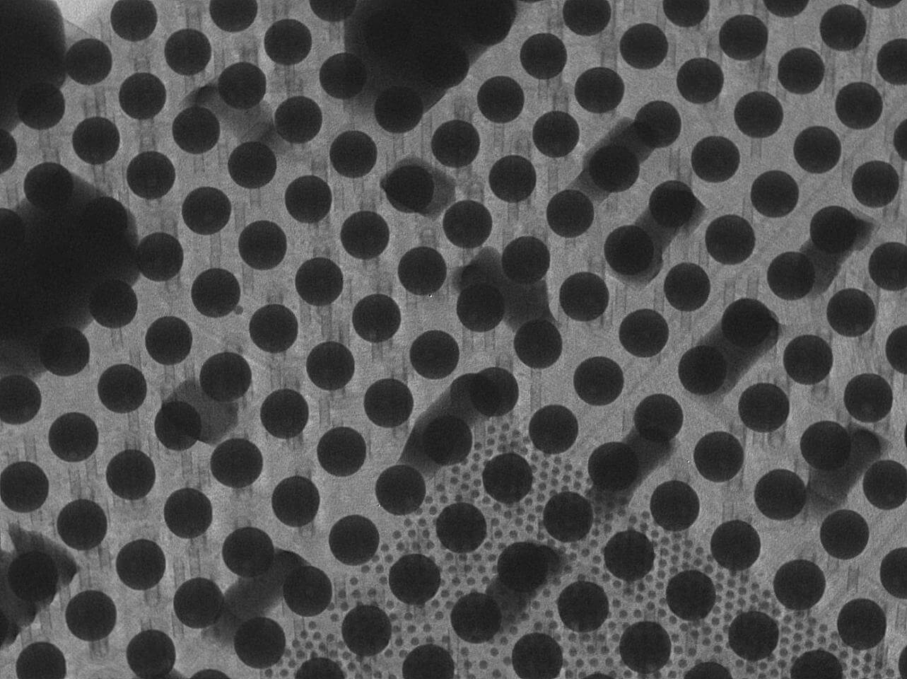
X-ray is non-negotiable on BGA boards. You cannot see solder joints under a BGA package — voids, bridges, head-in-pillow defects are invisible to optical inspection. And flying probe validates net connectivity without a custom test fixture — at 2,500 units/month, you cannot justify the fixture tooling cost that makes sense at 50,000+.
Nothing leaves the line without passing through three gates — and on HDI boards, every gate has teeth.
- Incoming Quality Control: High-Tg laminate gets Tg-certified at ≥170 °C before it touches the press. ENIG nickel/gold thickness is verified against IPC-4552B. Copper foil peel strength is checked. If the material is off-spec, it does not enter the line.
- In-Process Quality Control: Laser via drilling depth and diameter, sequential lamination registration, VIPPO fill integrity, plating uniformity — all monitored in real time. A deviation triggers an automatic lot hold.
- Outgoing Quality Control: 100% AOI, X-ray on every BGA position, electrical test, flying probe net continuity. No sampling. Every board goes through all four test methods.
For a device installed in a moving vehicle, one field failure costs more than a year of 100% inspection. That math is not complicated.
The pilot validated the full chain — HDI laminate procurement, sequential lamination, laser drilling, ENIG plating, and four-method inspection. 98.5% first-pass yield on 1,000 boards. Customer signed off on appearance quality. The program moved to 2,500 units per month.
The staged ramp — pilot first, pricing later — let a 30-person startup see real yield data before committing production capital. And PS Electronics’ throughput means the 2,500 monthly run never competes for line time during peak season.
For challenging HDI PCB projects like this, PCBCool serves as the digital online brand of PS Electronics, helping customers access engineering review, certified manufacturing, and multi-site production support for stable production.