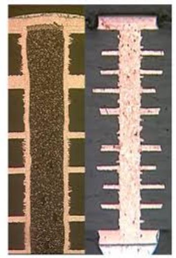
In 2024, I audited 29 failed BGA prototypes across Kenya, Bolivia, Vietnam, and Eastern Europe. In 22 cases, the schematic was correct, the layout passed DRC, and the Gerbers were clean—yet the board wouldn’t boot. X-ray and cross-section analysis revealed head-in-pillow defects, voided solder joints, misaligned microvias, and thermal warpage cracks.
The root cause wasn’t the assembler. It was physics.
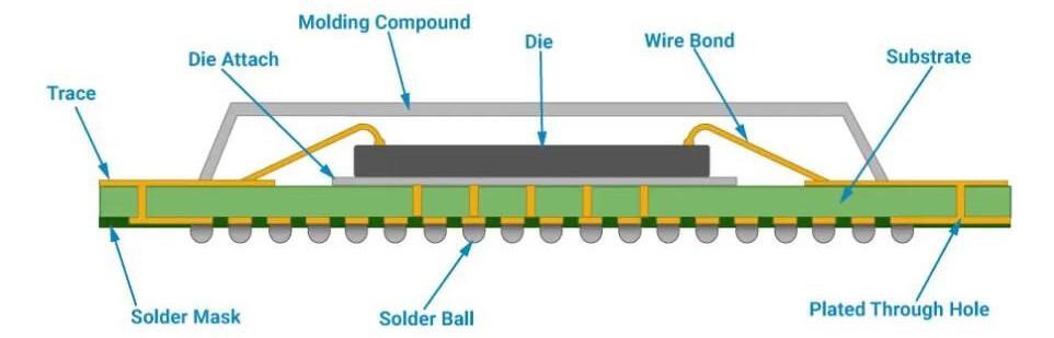
BGA isn’t just “dense routing.” It’s a co-design challenge spanning package architecture, stackup engineering, thermal management, signal integrity, reflow dynamics, and even regional climate. Get one element wrong—especially trace length balance inside escape routing and breakout regions—and you’re not just delaying a prototype. You’re often burning over $1,000 on X-ray diagnostics, hundreds more on rework, and weeks of credibility.
This guide delivers what actually works in production:
- Via-in-pad approaches that prevent solder wicking in high-humidity environments
- Fanout techniques matched to pitch, budget, and local fabrication capability
- Reflow-aware designs that avoid uneven solder collapse under low-pressure conditions
- How to audit your EMS partner’s BGA process before committing
No marketing fluff. No “just follow IPC.”
Just engineering that survives monsoons, altitude, lead-free reflow—and the unforgiving timing margins of modern high-speed interfaces.
Unfilled vias under BGA pads act as capillary channels during reflow, wicking molten solder away from the joint. In controlled, dry labs this often results in 30–50% voiding.
But in high-humidity environments—such as Nairobi (≈85% RH) or Bangkok (≈90% RH)—moisture trapped in unfilled vias flashes to steam at ~220 °C, violently expelling solder from the joint.
X-Ray Evidence:
A 0.4 mm pitch ESP32-WROVER module on a Kenyan IoT board showed an 85% void rate in corner balls. Cross-sectioning confirmed steam-induced solder blowout originating from via barrels.
Fix:
Specify filled and capped vias for all pads under BGA when pitch ≤ 0.5 mm.
But not all fills are equal:
- Copper-Plated Fill: Best thermal conductivity (~398 W/m·K), ideal for power and ground, but requires sequential lamination (~+30% cost)
- Epoxy Fill + Copper Cap: Good electrical continuity, moderate thermal (~3–8 W/m·K), sufficient for most signal BGAs
- Non-Conductive Epoxy: Avoid. Creates thermal bottlenecks and CTE mismatch
IPC-7351B recommends pad diameter ≈ 0.85 × ball pitch, but many designs ignore solder mask expansion—the clearance between the copper pad and mask opening.
In cost-optimized fabs (common in parts of Southeast Asia), solder mask alignment tolerance is typically ±0.1 mm. With zero expansion, the mask can partially encroach on the pad, leading to inconsistent wetting and head-in-pillow defects.
Recommended Practice:
- Pad diameter = 0.85 × pitch
- Solder mask opening = pad + 0.2 mm (+0.1 mm per side)
- Use NSMD pads by default; only specify SMD pads when explicitly required by the fabricator
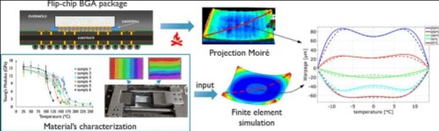
BGAs depend on symmetric thermal mass during reflow. If one side of the package sits over significantly more copper—such as a solid ground plane—it heats more slowly, inducing package warpage and cold joints.
At high altitude—La Paz, Bolivia (≈3,600 m)—atmospheric pressure drops to roughly 63 kPa. This reduces convective heat transfer and degrades solder paste outgassing. Standard sea-level reflow profiles often fail, resulting in incomplete solder coalescence.
Fix:
- Add copper thieving in inner layers beneath BGAs to balance thermal mass
- Maintain uniform plane distribution; avoid large asymmetric pours
- Share altitude-adjusted reflow profiles with your EMS partner:
- Soak Time: +15 s
- Peak Temperature: +5 °C
- Time Above Liquidus: ≥ 60 s
| Strategy | Best For | Fab Requirement | Risk |
|---|
| Perimeter Fanout | Pitch ≥ 0.8 mm (typical for many BGAs) | Standard 2-layer | Wastes center routing; not scalable |
| Dog-Bone | Pitch ~0.65 mm | 4+ layers, via next to pad (filled/capped if via-in-pad is used) | Requires precise via placement; risk of bridging |
| Staggered Microvia | Pitch 0.5–0.4 mm | HDI, laser drill | Cost increases ~2.5×; not available in Tier-3 EMS |
| Skip-Via (Nearest Neighbor) | Pitch 0.4 mm, pin-swappable | Layout flexibility | Only works if IC allows pin swapping or remapping |
Pro Insight:
For 0.4 mm pitch (ESP32, nRF52840), a microvia stack is ideal—but many EMS shops in Nairobi or Manila lack laser drilling capability. A practical fallback strategy is to use dog-bone fanout with via next to pad, with filled/capped vias, and accept 2–3 lost center pins.
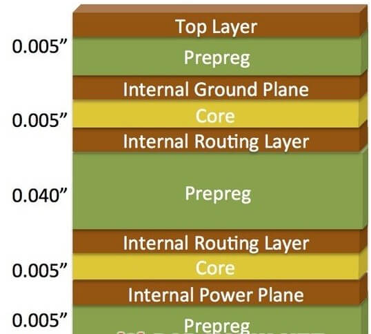
A BGA stackup must serve three masters: signal integrity, power integrity, and thermal conduction.
Recommended 6-layer stackup for 0.4–0.5 mm BGA:
- Top: Signal (BGA layer)
- Inner 1: Ground (solid, no splits under BGA)
- Inner 2: Power (split only outside BGA footprint)
- Inner 3: Power
- Inner 4: Ground
- Bottom: Signal
Prepreg thickness under the BGA: ≤ 0.1 mm (typical target for controlled impedance)
Core material: Isola FR408HR or Panasonic Megtron 6 for >1 Gbps signals
Avoid generic FR-4 for DDR3/4.
Use low-loss, low-Dk-variation laminates to prevent timing skew and impedance drift.
Even perfect designs fail in the field—because manufacturing conditions and environments vary. Make rework possible:
- Expose at least two diagonal corner balls — hot-air nozzles need access
- Place fiducials near the BGA (within ~5 mm when possible) — enables automated reballing and alignment
- Add testpoints on critical nets: RESET, BOOT, JTAG, clock
- Avoid metal shields directly over the BGA — they trap heat and block nozzle access
In rural Kenya, technicians often use manual hot-air stations (858D). If all corners are covered by caps or shields, rework becomes impossible and the board is scrapped.
Pro Tip:
Include a “Rework Access Zone” in your mechanical drawing:
“No components or tall parts within 3 mm minimum of BGA corners.”
Before sending Gerbers, ask your EMS provider these questions:
“What is your first-pass yield for 0.4 mm pitch BGA?”
→ Typical target: high 80s to low 90s%. Below ~85% is a red flag.
“Do you use nitrogen reflow for fine-pitch BGA?”
→ Strongly recommended. Air reflow increases oxidation and reduces wetting, especially on fine-pitch paste deposits.
“What stencil thickness do you use for 0.4 mm pitch?”
→ 0.1 mm is typical. 0.15 mm increases bridging risk.
“Can you provide X-ray and AOI reports on the first article?”
→ Non-negotiable for mission-critical builds.
“Do you support conductive-filled vias?”
→ If not, avoid via-in-pad for pitch ≤0.5 mm.
Real cost:
A team in Hanoi skipped this protocol—EMS used air reflow and a 0.15 mm stencil, resulting in 63% bridging on an ESP32-WROOM-32U. Total loss: $4,200.
| Region | Challenge | Design Response |
|---|
| East Africa (Nairobi, 1,800 m, 85% RH) | Moisture absorption, oxidation | Conductive-filled vias; acrylic conformal coating; avoid exposed copper |
| Andes (La Paz, 3,600 m) | Low convection, reflow issues | Reduce thermal mass under BGA; specify altitude-adjusted reflow profile |
| Southeast Asia (Bangkok, sea level, 90% RH) | Moisture-driven corrosion and dendrite risk | Improve cleanliness, increase creepage/clearance, consider conformal coating or potting |
| Eastern Europe (Budapest, industrial) | Vibration, thermal cycling | Add strain relief; use underfill for large BGAs (typical ≥10×10 mm) |
Pro Tip:
For tropical deployments, add a conformal coating step in your assembly notes.
“Apply acrylic conformal coating after ICT — cure 24 hrs @ 25°C.”
For BGAs >10×10 mm (e.g., FPGAs, processors), the CTE mismatch between PCB (~17 ppm/°C) and silicon (~2.6 ppm/°C) causes solder fatigue during thermal cycling.
Solution: capillary underfill (e.g., Henkel LOCTITE 3540):
- Can reduce stress by up to ~70%
- Can increase thermal cycle life from ~500 to several thousand cycles
- Commonly required or strongly recommended for automotive/industrial reliability targets
But underfill adds cost (~$0.80–$2.50 per unit) and complicates rework. Only use when:
- Operating temp range >60°C
- Board subject to vibration
- Product lifetime >3 years
BGA design isn’t about density—it’s about respecting physics across environments. The best BGA layouts aren’t the ones with the most routed signals. They’re the ones that account for humidity in Nairobi, altitude in La Paz, and the limitations of a technician’s hot-air station in a rural clinic. Design not just for the reflow oven—but for the field, the climate, and the human who must fix it when it fails. Because in hardware, reliability isn’t a spec—it’s a promise.
If you want to avoid costly re-spins and ensure your design survives real-world conditions, PCBCool can help. We offer BGA-aware PCB design, prototyping, and assembly, with production support in multiple regions to match your manufacturing reality.