While designing a printed circuit board, you are doing far more than creating a simple blueprint for component placement. You are also defining how easy—or how difficult—it will be to assemble that board in real-world production.
Design for Assembly (DFA) is the practice of designing PCB to be cost-effective, easy to assemble, and highly reliable during manufacturing. A well-executed DFA approach helps reduce assembly errors, shorten production time, and avoid unnecessary cost increases during PCBA.
By the end of this guide, you will understand how to apply DFA principles to design printed circuit boards that are optimized for efficient and reliable assembly, especially in practical PCBA projects.
Before starting circuit design, it is essential to understand how PCB are assembled. Most boards use Surface Mount Technology (SMT), where components are placed on pads and then soldered. If through-hole components are present, they are either hand-soldered or wave-soldered.
The simplified steps of a typical PCB assembly process include:
- Applying solder paste using a stencil.
- Placing components with a pick-and-place machine.
- Reflow soldering the solder paste.
- Inspecting the board and adding any through-hole components if required.
Each step has specific design requirements that must be considered during PCB layout to ensure efficient and reliable assembly.
At a basic level, the arrangement of components on the board directly affects assembly difficulty and cost.
Components should be grouped by type. Surface mount components should ideally be placed on one side of the board (preferably the top side). When using both sides, heavier components should be placed on the top side and lighter components on the bottom. This helps prevent components from falling off during the second reflow cycle.
Maintaining consistent component orientation is a key element. Polar components, such as diodes, electrolytic capacitors, and ICs, should face the same direction. Common practice is aligning all components so that pin 1 of each component faces the top-left corner of the board. This reduces pick-and-place programming time and placement errors.
Leaving adequate space between components is also important. As a guideline, maintain at least 0.5 mm between adjacent components. For components that generate heat, increase the spacing accordingly. Your assembly house will appreciate the extra clearance, and troubleshooting becomes much easier with proper spacing.
Pad geometry might seem straightforward, but getting it right is a very crucial factor for successful assembly.
Using manufacturer-recommended pad patterns whenever possible is a good practice. Generic footprints are provided by IPC-7351 standards for various package types.
For hand soldering, ensure that pads are slightly larger than the minimum requirement by adding an extra 0.2–0.3 mm to pad length for components like resistors and capacitors. This provides a larger target and improves the quality of the solder joint.
It is bad practice to add isolated copper fills under components where solder paste will be applied. This can cause tombstoning, a phenomenon where one end of the component lifts off the board during soldering.
You should place at least three fiducials on your board in an asymmetric pattern. It is recommended to place each fiducial near the corners of the board, with approximately 5 mm of clearance from the edge. Fiducials should be 1 mm diameter circular copper pads with no solder mask, surrounded by at least 2 mm of clearance free from copper and silkscreen.
For boards assembled on panels, it is a good practice to add panel-level fiducials in addition to board-level fiducials.
Include a tooling hole if the board will be panelized or requires precise positioning during assembly.
The silkscreen serves as a guide for assembly instructions. If applied correctly, it prevents errors; if not, it can cause confusion. It should not be placed over pads or vias, as most manufacturers will automatically remove silkscreen from these areas, which can result in partial markings.
Including a clear polarity indicator for every polarized component is recommended. For example, a bar can indicate the cathode of a diode.
Adding reference designators is also important. They should be positioned near the component, but not underneath it.
Adding key indicators such as board revision number, date code, and company logo allows tracking of board versions during production and deployment.
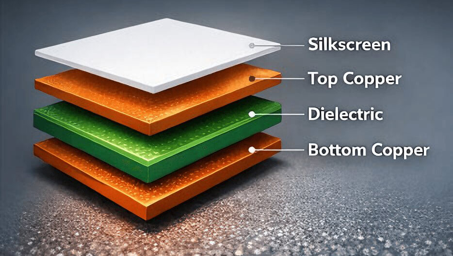
For multi-layer boards, the layer stacking arrangement significantly affects manufacturing and assembly.
For example, a typical 4-layer board stack is:
- Top Signal Layer
- Ground Plane
- Power Plane
- Bottom Signal Layer
Recommendations for good layer stacking include:
- Maintain symmetry during stacking. If a heavy copper layer is on top, it should be balanced with copper on the bottom layer to minimize board warping.
- Keep the layer count to what is necessary. A well-designed 2-layer board is generally preferable to a poorly designed 4-layer board.
Special considerations are required for heat-generating components.
Use heat relief connections for through-hole pads that connect to large copper areas. Without heat relief, the pads can act as heat sinks, preventing proper soldering. Heat relief connections use thin spokes to connect the pads to the copper plane, limiting heat dissipation to ensure successful soldering.
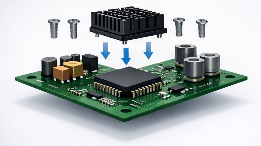
Additionally, using wide traces and thermal vias under IC thermal pads helps to efficiently spread heat generated by high-power components, improving reliability and performance.
Testing plays a crucial role in the debugging process. Including test points from the earliest stage of board design is recommended. Place test points for ground connections, key signals, and locations with critical voltages. They should be approximately 1 mm in diameter.
Additionally, ensure that test point placement does not interfere with programming headers such as JTAG or SWD, and that these headers remain easily accessible. Programming/debugging headers should be positioned away from other components for convenience.
Before sending your design files to the manufacturer, verify your design systematically using a checklist based on your requirements, ensuring it meets the manufacturer’s recommendations. A generic checklist could include:
- All components are assigned footprints matching the desired package.
- Polarity marking for polarized components.
- Fiducials are present and correctly placed.
- No overlaps in silkscreen, pads, or vias.
- Reference designators are present and readable.
- Board outline is on the correct layer.
- All layer files are present (Gerber, drill files, pick-and-place data).
- Minimum trace width complies with the manufacturer’s recommendations (6 mil / 0.15 mm is common).
- Via sizes are manufacturable (typically 0.3–0.5 mm).
- Hole-to-hole clearance is sufficient (at least 0.3 mm between holes).
- Hole-to-board edge clearance is sufficient (at least 0.5 mm from holes to board edge).
Design for Assembly (DFA) is not about memorizing rules and regulations, but about understanding the assembly process of circuit boards and making careful considerations that accommodate real-world manufacturing constraints.
Start implementing DFA in a simple way. Even a basic 2-layer board can benefit from these principles. By gaining experience, you will develop an intuition for what works best and what causes problems. Review assembly drawings from your manufacturer and, when you have your board in hand and encounter issues, analyze why they occurred and adjust your next iterations accordingly.
The best insights come from observing your boards’ assembly process. Each design teaches lessons about the relationship between what you have designed and what happens on the assembly line.
For engineers and designers seeking reliable PCB manufacturing and assembly services, PCBCool offers expertise in DFA-friendly production, helping you turn your designs into high-quality, manufacturable boards with minimal errors and maximum efficiency. Partnering with PCBCool allows you to focus on innovation while leaving the assembly challenges to professionals.