In situations where the schematic, layout, and functional behavior of an existing printed circuit board (PCB) are unknown, PCB reverse engineering provides a structured approach to analyze and understand the board. This practice is widely applied in maintenance, repair, redesign, migration, and documentation, rather than for mere duplication.
It is important to distinguish responsible reverse engineering from unauthorized cloning for commercial resale. The objective of professional reverse engineering is to gain insight into a system’s operation, support the maintenance of legacy equipment, or improve manufacturability, all while adhering to legal and ethical standards.
This guide outlines the step-by-step process of reverse engineering a PCB and demonstrates how to properly document and share the results, particularly within professional and manufacturing contexts.
Before initiating any PCB reverse engineering project, it is imperative to carefully consider the legal, ethical, and compliance implications. Not all PCBs may—or should—be reverse-engineered for distribution.
Key principles include:
- Respecting intellectual property and licensing agreements.
- Avoiding direct commercial cloning of proprietary PCBs.
- Clearly documenting the objective of the reverse engineering effort.
- Utilizing reverse-engineered data appropriately, such as for repair, education, internal reference, or process improvement.
In many professional contexts, reverse-engineered files are shared exclusively within the organization, or with partners under strictly controlled terms. Implementing disclaimers and version control helps mitigate legal risks and prevents potential misuse.
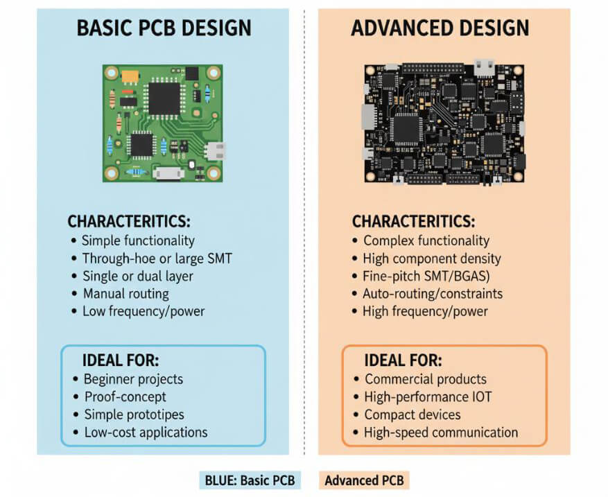
This step is critical for determining the complexity, time requirements, and overall feasibility of the project.
Key evaluation factors include:
- Number of layers (single, double, or multi-layer).
- Component density and package types.
- Presence of fine-pitch or BGA components.
- Availability of component datasheets.
- Board condition and readability.
At this stage, engineers define the project objective, such as:
- Gaining functional knowledge of the board,
- Creating a complete reproduction, or
- Conducting a redesign for manufacturability.
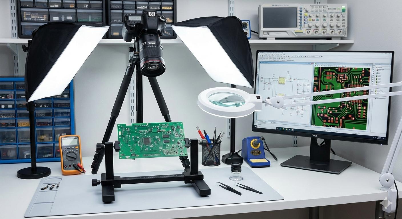
Essential Tools:
- High-resolution camera or flatbed scanner.
- Consistent lighting and a tripod.
- Computer equipped with image and vector editing software.
- Multimeter with continuity testing capabilities.
- Magnifying glass or microscope.
- PCB holder or jig.
Software Options:
- Image editors (e.g., GIMP).
- Vector design tools (e.g., Inkscape).
- EDA software (e.g., KiCad, Altium).
Process:
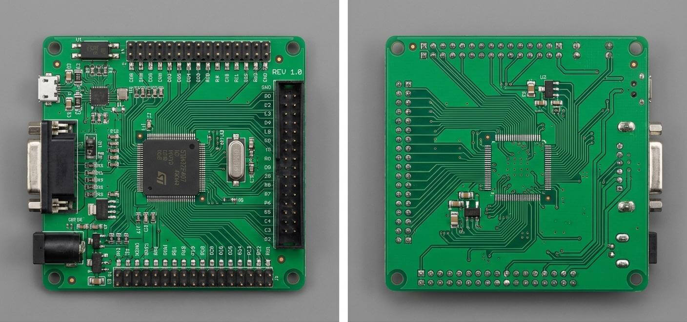
- Gently brush the PCB to remove dust, debris, or loose particles.
- Position the board flat and capture straight-on photographs, avoiding perspective distortion.
- Photograph the entire board as well as close-up images of densely populated areas.
- Capture both sides of the board using consistent lighting and focus.
Practical Tips:
- Use RAW photo mode when available to preserve image quality.
- Consider taking multiple overlapping images and stitching them together for a complete view.
Key Documentation:
- Record board orientation and connector locations.
- Label component reference designators clearly.
- Note silkscreen text, revision markings, and other identifiers.
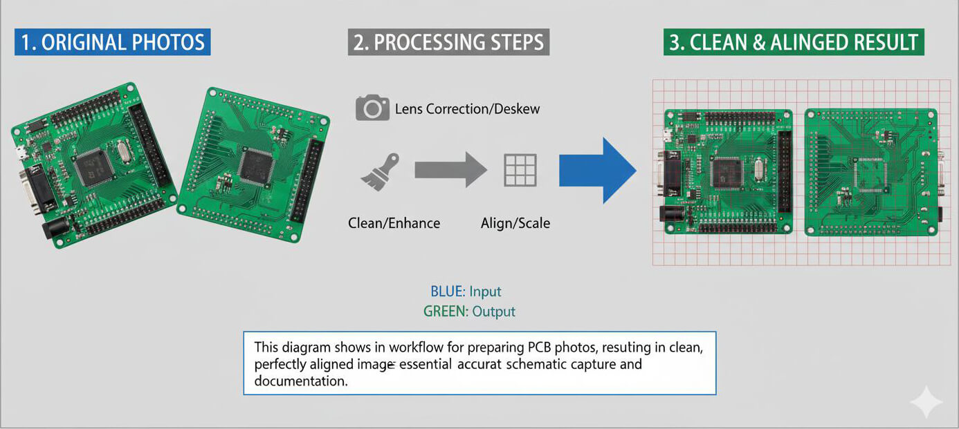
Process:
- Import the photographs into your preferred image editing software (e.g., GIMP).
- Straighten the PCB using guides and rotation tools to correct perspective distortion.
- Crop extraneous backgrounds to focus exclusively on the board.
- Eliminate shadows and reflections using blur, clone, or other correction tools.
Alignment for Tracing:
- Align images so that holes and pads overlap precisely when layered.
- Utilize alignment marks on the board, such as corners and mounting holes, to ensure accuracy.
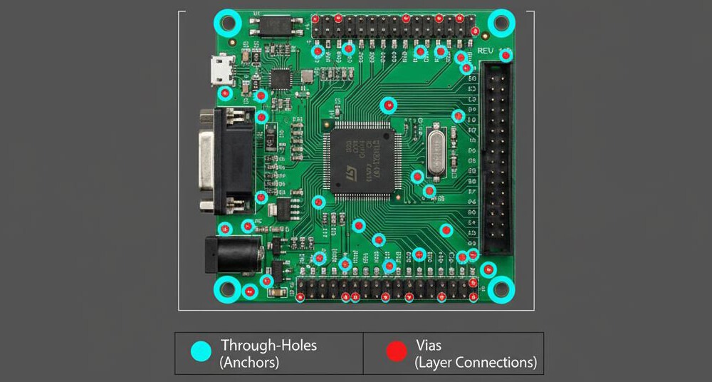
Key Actions:
- Mark all visible through-holes and vias on a dedicated layer in your image or vector editor.
- Use consistent symbols (such as dots or circles) to represent through-connections, facilitating clarity during the tracing process.
Practical Tip:
If lighting or contrast hinders visibility of holes or pads, adjust color channels in your image editor (e.g., disable green and blue channels to better isolate copper pads).
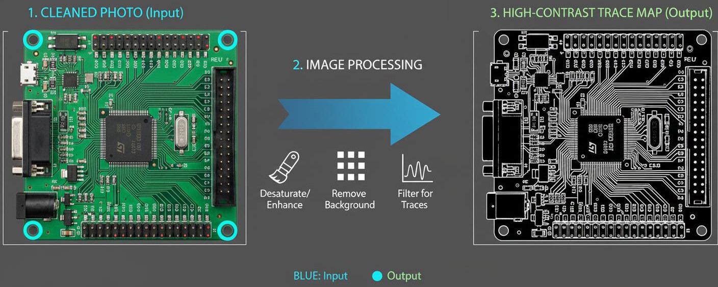
Process:
- Convert the image to grayscale to simplify the visual data.
- Enhance contrast so that copper paths are clearly distinguishable from the board substrate.
- Adjust levels to render copper traces as near-black on a white background.
- Manually remove text, logos, silkscreen markings, and other artifacts that could interfere with trace recognition.
Outcome:
The resulting cleaned image should display only the copper geometry.
Process:
- Use a centerline tracing tool (e.g., AutoTrace) to convert pixel-based images into vector paths.
- Save the traced output in a standard vector format such as SVG for subsequent editing.
Fine-Tuning and Editing:
- Open the SVG file in a vector editor (e.g., Inkscape).
- Remove extraneous nodes and smooth trace lines to improve clarity.
- Correct any misaligned segments to ensure connectivity is accurately represented.
Process:
- List all components along with their reference designators.
- Consult datasheets using component markings to verify specifications.
- Confirm key characteristics, including power pins, input/output pins, and primary functionality.
Handling Unclear Markings:
- Cross-reference package size and pin count to narrow down possible component types.
- Use continuity testing to verify suspected connections and functional pins.
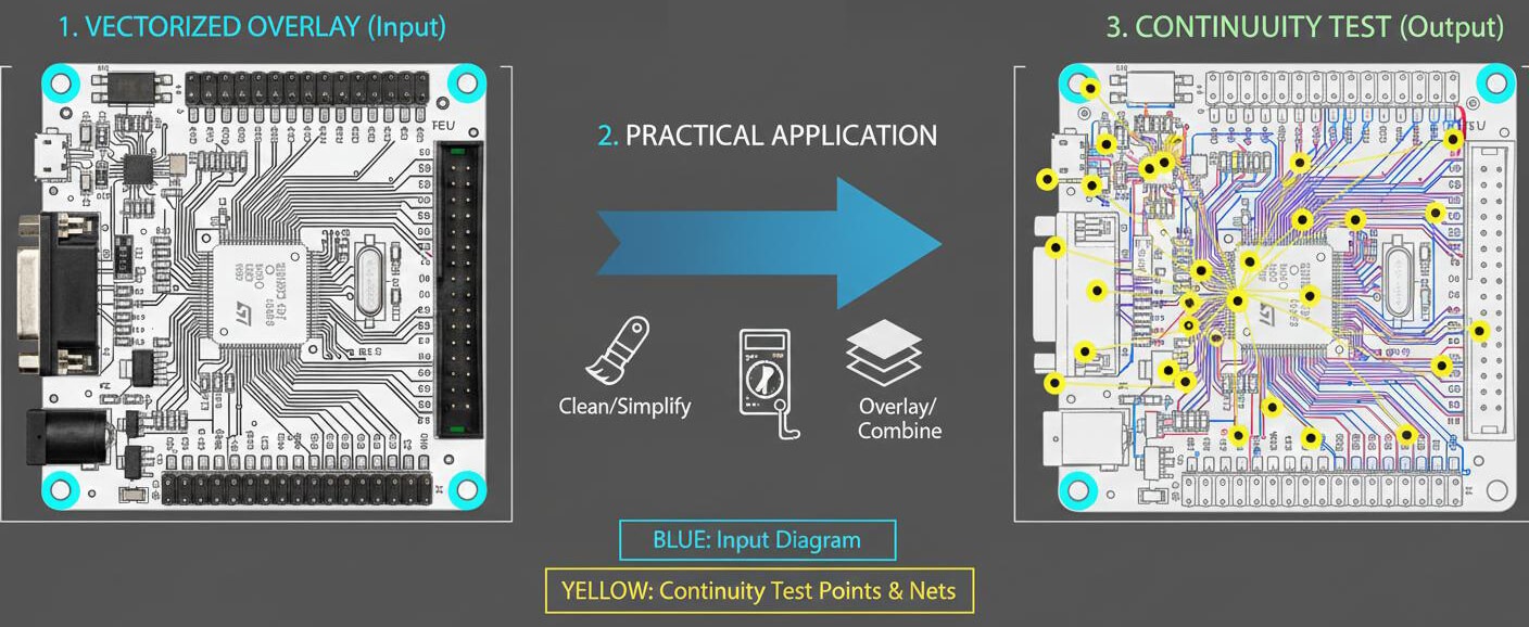
Process:
- Set the multimeter to continuity mode.
- Probe between pins and pads to confirm electrical connections.
- Document confirmed connections directly on your vector map or schematic draft.
Practical Tips:
- For nets that span both sides of the PCB, use consistent names, labels, or color coding to avoid confusion.
- Maintain a clear legend or key for colors and symbols to ensure traceability throughout the schematic reconstruction process.
Process:
- Place all components according to their reference designators.
- Connect nets based on continuity testing results and vector trace data.
- Add power rails and ground connections early to establish a reliable framework.
- Organize the schematic into functional blocks, such as analog, digital, and power sections.
- Visually validate connections against the original PCB to ensure accuracy.
Practical Tips:
- For complex boards, consider using hierarchical sheets to simplify design organization and improve readability.
- Maintain consistent labeling and annotation throughout the schematic for traceability and clarity.
Validation Checks:
- Visually match net connections between the schematic and the PCB layout.
- Confirm power distribution, including voltage rails, grounding, and decoupling paths.
- Verify reference designators to ensure component placement and identification are consistent.
- Cross-check critical signal paths, such as clocks, communication lines, and control signals.
Functional Confirmation:
- When feasible, power the board under controlled and safe conditions and observe its behavior.
- Confirm that the board’s operation matches the functional expectations derived from the schematic.
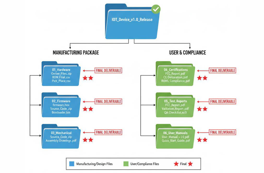
Deliverable Includes:
- Final schematic files (e.g., .sch), clearly reflecting verified connectivity.
- Bill of Materials (BOM) with accurate manufacturer part numbers and key specifications.
- Annotated PCB images, including component labels, orientations, and key reference points.
- Trace maps and net names that document signal flow and electrical relationships.
Compliance and Documentation Notes:
- For non-commercial or internal use, include a clear disclaimer outlining the project’s purpose, scope, and respect for intellectual property (IP).
- Maintain consistent file naming, version control, and revision notes to support traceability.
PCB reverse engineering is a powerful engineering practice that, when executed correctly, delivers far more than a simple reproduction of an existing design. Through a systematic workflow, careful validation, and responsible documentation, engineering teams can effectively maintain legacy systems, improve reliability, and support manufacturing continuity—without compromising ethical or legal standards.
For organizations seeking to turn reverse engineering results into practical manufacturing outcomes, working with an experienced PCB partner is essential. PCBCool supports engineers and businesses by providing PCB fabrication, assembly, and engineering-aware manufacturing services, helping ensure that reverse-engineered designs can be validated, produced, and scaled with confidence.