Wire bonding has long been the cornerstone of semiconductor packaging, widely recognized for its reliability and established process. However, despite its maturity, achieving consistently high yield and controlling manufacturing costs remain ongoing challenges for many production lines.
The performance and cost of wire bonding are largely determined before production even begins. Decisions made during die design, substrate layout, material selection, and pad configuration can have a profound impact on bond quality, cycle time, and failure rates. Even seemingly minor design choices may introduce significant production difficulties if not carefully considered.
In this article, we will explore practical strategies that help engineers and manufacturers optimize wire bonding processes—improving yield, reducing defects, and ultimately lowering costs—without compromising reliability.
Wire bonding is the process of establishing both electrical and physical connections between a semiconductor device and its package substrate using extremely fine metal wires. Typical wire diameters range from 15 to 75 microns, and successful bonding relies on a combination of pressure, heat, and ultrasonic energy.
From a manufacturing perspective, wire bonding is a serial process: each connection is formed individually, which means the total bonding time scales directly with the number of I/O connections. Consequently, bond count is a primary factor influencing assembly cost, cycle time, and equipment utilization.
There are two widely adopted wire bonding techniques:
- Ball Bonding: Commonly used with gold or copper wires, forming a spherical bond at the wire tip.
- Wedge Bonding: Typically employed with aluminum wires, using a wedge-shaped tool to form the connection.
Each method comes with distinct processing requirements, cost implications, and reliability characteristics. Selecting the appropriate bonding technique is not merely a matter of engineering preference; it requires aligning material performance with design constraints to ensure optimal yield, efficiency, and reliability.
Gold wire has long been the industry standard due to its excellent ductility and resistance to oxidation. From a manufacturing perspective, it provides a wide process window and consistently high first-pass yield, making it suitable for mixed or lower-volume production.
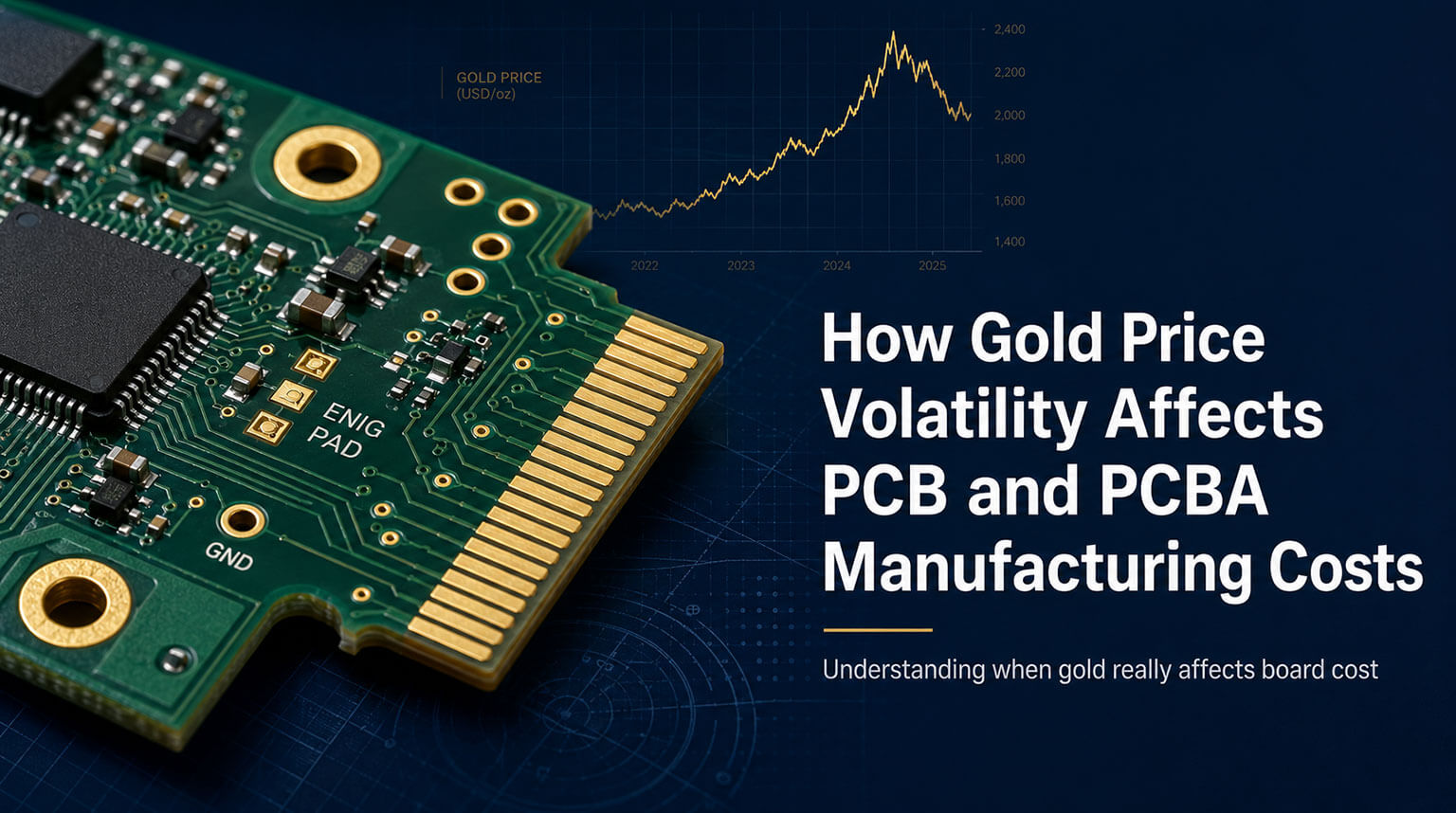
However, the cost of gold is volatile and can significantly impact assembly expenses, particularly in high pin-count devices. Additionally, the formation of gold-aluminum intermetallic compounds at the bond interface may pose long-term reliability concerns if not properly managed.
Gold wire remains a viable choice where reliability and process margin are top priorities, but it is increasingly difficult to justify for cost-sensitive products.
Copper wire has gained popularity as a lower-cost alternative to gold. It offers superior electrical conductivity and improved resistance to electromigration while reducing raw material costs.
From a manufacturing standpoint, copper bonding requires tighter process control, including:
- Higher bonding force
- Narrower ultrasonic energy windows
- Increased sensitivity to surface oxidation
Meeting these requirements demands precise equipment calibration and strict control of environmental conditions. When properly implemented, copper wire bonding can be both cost-effective and reliable. However, it is less forgiving regarding pad metallization contamination, making early DFM alignment essential.
Aluminum wire is primarily used in wedge bonding and is common in power devices and specific automotive applications. It provides good compatibility with aluminum pads and avoids some intermetallic issues associated with gold.
Nevertheless, aluminum wire has limitations, including lower bonding speed and inability to support fine-pitch packaging. It is best suited for applications where bond integrity is more critical than density.
Ball bonding is the predominant method in modern IC packaging, supporting high bonding speeds and fine-pitch interconnects. The process begins by forming a free air ball at the wire tip, which is then bonded to the die pad before completing the second bond on the substrate.
From a manufacturing perspective, ball bonding offers several advantages:
- High throughput
- Compatibility with automated, high-volume production
- Excellent repeatability for dense I/O layouts
This method is particularly well-suited for consumer electronics, microcontrollers, and high-pin-count devices, where cycle time and cost per unit are critical factors.
Wedge bonding forms connections by pressing the wire directly onto the pad using ultrasonic energy, without forming a ball. This technique allows for precise bond placement and is effective for non-planar surfaces or specialized substrates.
Although slower than ball bonding, wedge bonding provides benefits in applications that require:
- Larger wire diameters
- Multiple bond directions
- Enhanced mechanical robustness
The selection between ball and wedge bonding should not be based on familiarity or legacy practices. Instead, it must align with design constraints, material compatibility, and production volume to ensure reliable and cost-effective assembly.
The dimensions and layout of bond pads play a key role in bond strength and placement accuracy. Pads that are too small increase the risk of non-sticks and lifted bonds, whereas oversized pads consume valuable die area and restrict routing density.
From a manufacturing perspective, maintaining consistent pad geometry across the die simplifies process optimization and enhances yield. Variability in pad size or placement often requires conservative process settings, which can reduce bonding speed and elevate defect rates.
Successful wire bonding also depends on metallurgical compatibility between the wire and pad surfaces. Common pad finishes include aluminum, aluminum-copper alloys, and nickel-based stacks. Incompatible material combinations can result in poor bonding, excessive intermetallic formation, or long-term reliability issues.
Ensuring metallization compatibility is most effective when addressed early in the design phase, with collaboration among design, fabrication, and assembly teams across the supply chain.
The geometry of wire loops affects mechanical integrity and process robustness. Excessively tall loops are susceptible to vibration damage and wire sweep during encapsulation, while loops that are too low can cause short circuits or localized stress concentrations.
From a manufacturing perspective, maintaining stable loop profiles reduces process variation during encapsulation and contributes to higher overall assembly yield.
Wire length also directly influences electrical characteristics such as inductance and resistance. Longer wires can degrade signal integrity in high-speed or high-current applications. By optimizing die placement and pad arrangement to minimize wire length, manufacturers can achieve improved electrical performance and thermal reliability without incurring additional material costs.
Each additional bond increases cycle time, equipment wear, and potential failure points. Thoughtful system architecture that eliminates unnecessary I/O connections can substantially lower assembly cost while improving overall reliability.
The true cost of assembly reflects expected yield. Designs that push the limits of bonding—such as tight pad pitches, marginal metallization, or excessive loop heights—tend to increase defect rates. Rework and scrap costs are inherently embedded in the unit price.
High-yield designs move more efficiently through production, consume fewer resources, and scale more predictably, demonstrating that prioritizing yield and manufacturability is as important as achieving functional performance.
Wire bonding continues to offer unmatched cost efficiency and flexibility for a wide range of semiconductor applications. However, it is not always the optimal solution. Designs that demand very high frequencies, extremely high I/O counts, or strict form-factor constraints may require alternative interconnect methods, such as flip-chip. Careful evaluation is therefore essential.
The decision to use wire bonding should be driven by performance, reliability, and production requirements—not simply by familiarity or availability. Selecting the appropriate interconnect technology early in the design process ensures that the final assembly meets both functional and manufacturing objectives efficiently.
Wire bonding is far more than a legacy packaging technique. It is a mature, highly optimized manufacturing process whose success depends on careful alignment between design intent and production reality. Material selection, bonding methods, pad design, loop control, and yield optimization all interact to determine final cost, reliability, and manufacturability.
For engineering teams, hardware startups, and production engineers, the goal should not be to maximize density or minimize material cost in isolation. Instead, the focus should be on developing a wire bonding solution that delivers consistent yield, predictable performance, and scalable manufacturing.
Achieving this level of alignment requires not only expertise but also access to reliable manufacturing partners who understand the nuances of wire bonding. At PCBCool, we specialize in providing comprehensive PCB assembly and wire bonding solutions, supporting our clients from design for manufacturability to high-volume production. By combining technical guidance with robust process control, PCBCool helps ensure that wire bonding projects achieve the highest yield and cost efficiency.