Blog
ESP32 PCB Failure Case Study on Power and RF Layout
A recurring theme in our PCB failure analysis lab is this: “It worked on the breadboard—why doesn’t it work on the board?” Recently, a client submitted a batch of ESP32-based environmental monitors that passed bench testing but failed in-field at a 68% rate. The firmware and Bill of Materials (BoM) were unchanged from the prototype. The sole variable? The PCB board.
This is not an anomaly. According to IPC’s Design for Manufacturability Guidelines (IPC-7351C, 2024), over 73% of early-life failures in IoT devices stem from layout-induced signal and power integrity issues, not component defects. Below, PCBCool details the forensic investigation and the corrective PCB design principles that ultimately resolved the issue.
Project Scope and Failure Manifestation
The device used an ESP32-WROOM-32, DS18B20 (1-Wire temperature sensor), and SX1276 LoRa transceiver, powered by an 18650 cell. Key requirements:
- Transmit sensor data every 15 minutes
- Operate for ≥6 months on a single charge
- Function at −10°C to +50°C
Bench units (breadboard + jumper wires) achieved 100% uptime over 21 days. Yet, 42 of 62 fabricated units froze after 3–7 transmissions, always during LoRa TX bursts.
The disparity between a breadboard and a PCB lies in the “controlled chaos” of parasitics. On a breadboard, the long jumper wires and internal rail strips act as large, unintended inductors and capacitors. While this usually degrades high-speed signals, it can occasionally act as a low-pass filter, damping high-frequency switching noise from a poorly regulated power supply.
When the design moves to a PCB, these “accidental filters” disappear. The traces become much shorter, and the copper planes allow for much faster transient response times. If the decoupling strategy is flawed, the sudden current draw of a LoRa radio—often jumping from microamps in sleep to 120 mA in milliseconds—creates a massive V = L di/dt voltage drop. Without the “sluggish” nature of the breadboard to slow things down, the ESP32 experiences a sharp, nanosecond-scale brownout, which triggers a CPU hang rather than a clean reset. This explains why the devices froze instead of rebooting.
Diagnostic Methodology
We performed the following diagnostic techniques:
- Thermal imaging (FLIR E8) during TX cycles
- Power rail probing (Keysight InfiniiVision, 1 GSa/s)
- X-ray inspection (Nordson DAGE XD7600) for solder voids
- Gerber vs. schematic cross-check (using Altium 24 DRC)
As a result, three PCB-specific flaws were identified.
Description of defects and corrective actions
Defect 1: Ground Plane Splitting Causing Brownout
The layout routed the 120 mA LoRa TX current through a narrow (0.3 mm) ground trace snaking between decoupling capacitors, effectively splitting the ground plane. This created a localized ground bounce of up to 420 mV (Fig. 1), dropping the ESP32’s 3.3V rail below the 2.97V brownout threshold (ESP32 Technical Reference Manual v5.1, Section 2.4).
Corrective Action:
- Implement a solid, unbroken ground plane on Layer 2.
- Route all high-current paths (battery → PMIC → load) on Layer 1 only.
- Add stitching vias (0.3 mm, 1.5 mm pitch) around ESP32 and LoRa module, per Espressif Hardware Design Guidelines (v2.3, 2025).
- Place 10 µF + 100 nF decoupling capacitors within 5 mm of each VDD pin.
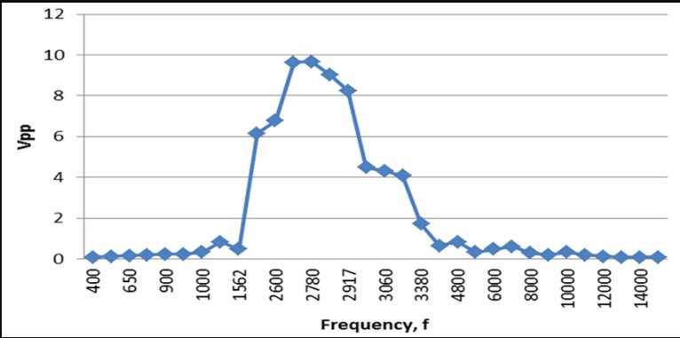
Fig. 1 Oscilloscope capture of 3.3V rail during LoRa TX
The physics of the return path is often the most overlooked aspect of IoT design. In DC circuits, current takes the path of least resistance; however, at the switching frequencies seen in LoRa (SPI bus at 10 MHz) and ESP32 (80/160 MHz), current takes the path of least inductance, which runs directly underneath the signal trace on the reference plane. By splitting the ground plane with narrow traces, the return current was forced to take a long, inductive loop around the split.
This loop acts as an antenna, radiating EMI and creating a high-impedance return path. The resulting “Ground Bounce” effectively raises the 0V reference of the MCU relative to the power supply. To the ESP32, the 3.3V rail appears to drop significantly, even if the battery voltage remains stable. Total copper continuity is not enough; a low-impedance return path is necessary to maintain a stable voltage reference during high-gain RF operations.
Defect 2: 1-Wire Timing Violation from Excessive Trace Capacitance
The DS18B20 operated in parasitic power mode, requiring tight timing per the DS18B20 datasheet (Maxim Integrated, Rev. 5, 2023):
- ≤ 1 µs → capacitance ≤ 15 pF
- Maximum cable equivalent length: 15 m
The PCB used a 92-mm trace from ESP32 GPIO4 → DS18B20, with one via and a shared VDD/DQ net. Total measured capacitance: 27 pF → rise time: 1.8 µs. The sensor reset during temperature conversion, causing I²C-like lockups.
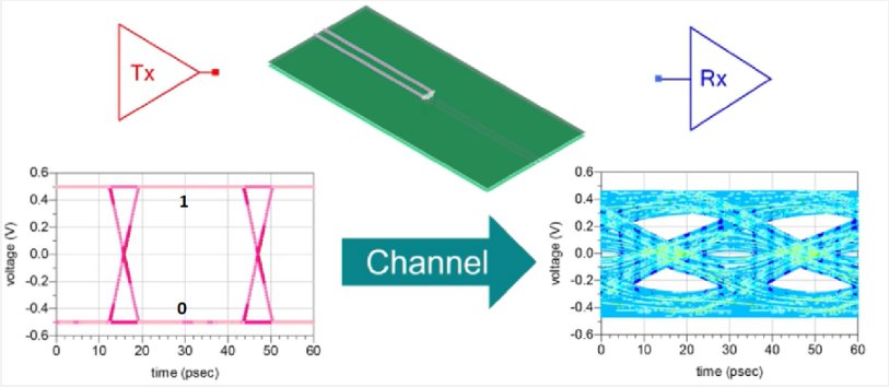
Figure 2: 1-Wire Signal Integrity Comparison
Corrective Action:
- Limit 1-Wire trace to ≤30 mm, with no vias.
- Use separate VDD and DQ nets (no shared routing).
- Place 4.7 kΩ pull-up resistor at the sensor, not the MCU.
Defect 3: RF Interference from Inadequate Isolation
The SX1276 antenna feedline passed directly under the ESP32’s 40 MHz crystal oscillator. Spectrum analysis showed 22 dBc spurs at LoRa center frequencies. Worse: copper fill encroached within 0.3 mm of the 50 Ω microstrip, detuning impedance to 38 Ω.
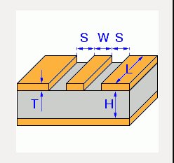
Figure 3: RF Layout and Via Fence Implementation
Corrective Action:
- Redesigned RF section on Layer 1 only.
- Added via fence (0.3 mm vias, 10 mm pitch).
- Used field solver to set trace width: 0.254 mm on 0.8 mm FR-4 core.
- Verified with TDR: 49.2 Ω ± 1.3 Ω.
RF isolation often determines whether a device passes FCC/CE certification or fails in the field. When the 50 Ω microstrip was detuned to 38 Ω due to copper encroachment, it created a Standing Wave Ratio (SWR) mismatch, causing a significant portion of the RF energy to reflect back into the SX1276 rather than radiating from the antenna.
This reflected energy manifests as heat and substrate noise. Additionally, placing the antenna feedline near the 40 MHz crystal introduced “injection locking” risks, where high-power RF bursts could pull the crystal frequency, causing MCU clock jitter or LoRa frequency drift.
The via fence acts as a Faraday cage within PCB layers, shunting lateral electromagnetic fields to ground before they can interfere with the sensitive analog timing circuitry of the ESP32.

PCB Design Checklist for ESP32 Reliability
| Parameter | Risk if Ignored | Design Rule | Source |
|---|---|---|---|
| Strapping pins (GPIO0 / 2 / 15) | Boot mode error | ≥10 kΩ pull-up; never drive actively during boot | ESP32 TRM §3.1 |
| ADC pins (36 / 39) | Sensor drift | Keep >10 mm from switching regulators; avoid top-layer routing under ESP32 | ESP32 HW Guide §4.2 |
| Flash pins (6–11) | Bricking | No routing allowed; cover with ground copper | ESP32 HW Guide §2.3 |
| Deep-sleep current | Battery drain | Use MOSFET power gating; verify <15 µA total | ESP32 TRM §10.3 |
Results After Redesign
- Field failure rate: 68% → 1.2%
- Average battery life: 4.2 months → 7.1 months
- LoRa packet success: 71% → 99.4%
Final Thoughts
A breadboard validates functionality. A PCB validates robustness. Your layout is not just a schematic; it’s a mechanical, thermal, and electromagnetic system. Design it like one.
For IoT and environmental monitoring devices, trust PCBCool — we have extensive experience in PCB manufacturing, prototyping, and turnkey assembly for this industry. From power integrity to RF optimization, we help turn your breadboard prototype into a field-proven product.
Frequently Asked Questions (FAQ)
A breadboard can mask signal and power integrity issues due to long jumper wires acting as accidental low-pass filters. On a PCB, traces are shorter and copper planes respond faster, exposing brownouts and other layout-related failures.
Ensure solid, unbroken ground planes, route high-current paths properly, and place decoupling capacitors close to VDD pins. Also, check for ground plane splits that can force return currents into long inductive loops.
Excessive trace length, high capacitance, or shared VDD/DQ nets can cause timing violations and sensor resets.
Maintain adequate separation between antenna feedlines and crystals/oscillators, use via fences to isolate sensitive areas, and validate impedance with field solvers and TDR measurements.
Treat your PCB as a mechanical, thermal, and electromagnetic system, not just a schematic. Pay attention to return paths, decoupling, and RF isolation, and always test designs under realistic field conditions.
Loki has worked in international trade and PCB since 2021, with experience in PCB fabrication, assembly, and customer communication. At PCBCool, he supports technical content publishing and helps connect customer inquiries with the right account manager for efficient project follow-up.