As electronic systems continue to evolve toward higher power density, greater reliability, and increased integration, traditional standard copper PCB (1–2 oz) are becoming increasingly inadequate for handling both high current loads and thermal stress.
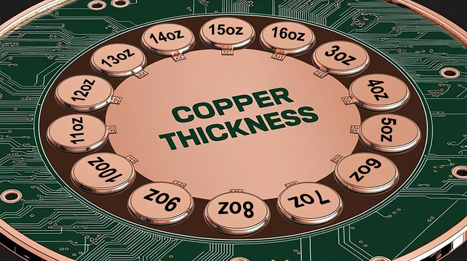
Heavy copper PCB (typically defined as ≥3 oz, where 1 oz ≈ 35 μm) have emerged as a critical substrate for high-power applications due to their superior current-carrying capacity, excellent thermal conductivity, and long-term reliability. They are now widely regarded as an essential infrastructure material in sectors such as electric vehicles, photovoltaic energy storage, and industrial power systems.
Unlike the broader PCB market, which is experiencing moderate growth, the heavy copper PCB segment is undergoing a structural expansion phase. This growth is driven by the convergence of three key factors: surging downstream demand, maturation of manufacturing processes, and optimization of production capacity. This article provides a comprehensive analysis of the global heavy copper PCB market, including current status, key drivers, regional dynamics, and a ten-year growth outlook.
According to the latest data from multiple authoritative institutions (including Global Growth Insights, QYResearch, and Verified Market Reports), the global heavy copper PCB market was valued at approximately USD 2.495 billion in 2025.
Although this represents only about 4% of the total global PCB market (estimated at USD 60–70 billion), its growth rate significantly exceeds the industry average.
- 2023: ~USD 1.975 billion
- 2024: Exceeds USD 2.2 billion (YoY growth ~11.4%)
- 2025: USD 2.495 billion (YoY growth >10%)
The heavy copper PCB market exhibits a “mid-heavy structure” with the fastest growth in ultra-thick copper:
- 3–6 oz (Mainstream): ~65% share
Widely used in automotive OBCs, industrial inverters, and PV inverters, offering the best balance between cost and performance.
- 2–3 oz (Entry-level upgrade): ~20% share
Applied in server power supplies and communication modules as an upgrade from standard PCB.
- ≥10 oz (High-end): ~15% share, but CAGR >12%
Used in 800V EV platforms, energy storage converters, and rail traction systems, featuring the highest technical barriers and pricing.
Heavy copper PCB are highly concentrated in high-power applications, with two sectors accounting for over 70% of demand:
- Electric Vehicles (EVs): Largest segment (~35%–40%)
The transition to 800V architectures and adoption of SiC devices are driving the widespread use of 4–10 oz copper in motor controllers, OBCs, BMS, and DC/DC systems.
High-end EVs can use up to 1.45 m² of heavy copper PCB per vehicle.
- Renewable Energy & Power Electronics: (~30%–35%)
PV inverters, energy storage PCS, and wind converters are upgrading to 1500V–3300V systems.
For example, 8 oz copper PCBs can reduce IGBT operating temperature rise from 65°C to 42°C, extending module lifespan to 15 years.
- Industrial Control & Communications: (~20% combined)
Includes servo drives, 5G base station power amplifiers, and data center server power backplanes.
- Aerospace & Medical: (~5%–10%)
High-reliability, radiation-resistant, and wide-temperature applications with high unit value but lower volume.
Heavy copper PCB are not simply “thicker copper layers,” but rather integrated solutions combining materials, processes, and application engineering. Their growth is underpinned by long-term structural trends rather than short-term market cycles.
- Voltage Platform Shift: Transition from 400V to 800V doubles current density, making traditional 2 oz PCB insufficient due to overheating and reliability issues.
- SiC Adoption: Third-generation semiconductors increase thermal density by 30%–50%, requiring efficient heat dissipation enabled by thick copper.
- Safety Standards: ISO 26262 functional safety requirements demand zero-defect reliability; heavy copper offers lower resistance and longer thermal cycling life.
- Higher Power Levels: PV inverters scaling from 500 kW to 3.5 MW; energy storage systems from 100 kWh to 5 MWh, with currents exceeding 1000 A.
- Harsh Environments: Equipment must operate reliably for 25 years under -40°C to 85°C, high humidity, and salt spray conditions.
- Policy Support: Under global carbon neutrality targets, annual PV installations are expected to reach 520 GW by 2030, driving heavy copper PCB demand in inverters.
Historically, adoption was limited by manufacturing complexity and cost. Recent breakthroughs have unlocked growth potential:
Material Innovation:
- HVLP (ultra-low profile) copper foil (Rz < 1.5 μm) improves signal integrity
- High Tg (≥180°C) and high thermal conductivity (≥1.2 W/m·K) substrates enhance thermal performance
Process Advancements:
- LDI (Laser Direct Imaging) + selective plating enable 50/50 μm line precision
- Step copper lamination improves bonding between thick and thin copper layers
- Embedded copper structures enable in-layer heat dissipation, increasing power density by 40%
Manufacturing Upgrades:
- Automation has increased yields from ~65% to over 90%, while reducing unit costs by ~23%
Based on the latest forecasts (2026), the global heavy copper PCB market is expected to grow at a CAGR of 7%–8.5% from 2026 to 2035, significantly outpacing the general PCB market (~4.5%).
| Year | Market Size (USD Billion) | Growth Rate | Key Drivers |
|---|
| 2026 | 2.707 | 8.5% | EV 800V adoption, energy storage boom |
| 2027 | 2.937 | 8.5% | PV growth, industrial recovery |
| 2030 | 3.37–3.85 | 7.5%–8.0% | >60% renewable penetration |
| 2035 | 5.637 | 8.49% | Full-scale electrification |
- Electric Vehicles: CAGR 12%–15% (2026–2030)
Global EV sales expected to exceed 40 million units by 2030, with near 100% heavy copper PCB penetration.
- Renewable Energy: CAGR 10%–12%
Energy storage becomes the primary growth driver, with global installations reaching 1000 GWh by 2030.
- Ultra-Thick Copper (≥10 oz): CAGR >12%
Driven by 800V EV platforms, high-power inverters, and AI server power systems.
The global market shows a clear pattern of “Asia-Pacific concentration, China leadership”:
China, Japan, and South Korea dominate. China alone accounts for over 50% of global demand and production.
Strong growth (CAGR ~8.8%) driven by EVs and wind power; key player includes AT&S.
Stable demand from aerospace, defense, and high-end industrial sectors; key players include TTM and Isola.
Despite strong growth prospects, several risks remain:
- Raw Material Volatility: Copper accounts for 30%–40% of costs; price fluctuations impact profitability.
- High-End Capacity Barriers: ≥10 oz and high-layer-count heavy copper PCB remain concentrated among leading manufacturers.
- Alternative Technologies: DBC (Direct Bonded Copper) and AMB (Active Metal Brazing) ceramic substrates compete in ultra-high-power applications such as SiC modules.
Heavy copper PCB have evolved from a niche segment into a foundational technology supporting the global transition toward renewable energy and industrial digitalization. Their growth is fundamentally driven by the electrification of energy systems and the increasing power density of electronic devices.
For industry players, this represents both a technological upgrade cycle and a capacity expansion window. Companies that master advanced thick copper processes and establish partnerships with leading OEMs will be best positioned to capture opportunities in this new wave of high-power electronics innovation.
As a leading heavy copper PCB manufacturer, PCBCool is well-positioned to support this transition. We are capable of producing ultra-thick copper PCBs with copper weights up to 33 oz, meeting the stringent requirements of high-current and high-power applications.
Beyond fabrication, PCBCool offers turnkey EMS (Electronics Manufacturing Services), covering the entire product lifecycle—from PCB design and engineering support to component sourcing, assembly, and full system integration. This end-to-end capability enables our customers to accelerate time-to-market while ensuring performance, reliability, and cost efficiency.