
Related Articles
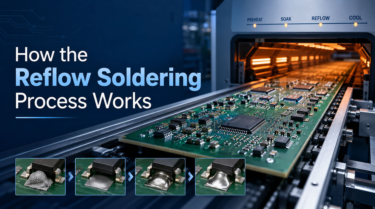
How the Reflow Soldering Process Works in SMT Assembly
The reflow soldering process turns solder paste into reliable PCB joints in SMT assembly. This guide explains how profile control, inspection, and process stability affect solder quality.
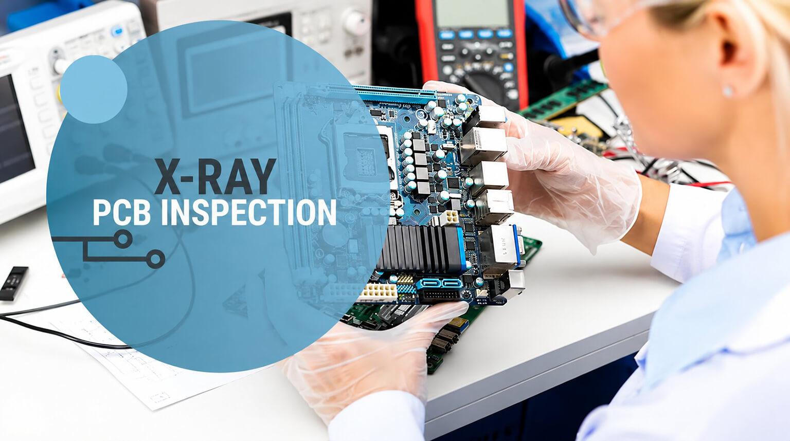
What Is PCB X-Ray Inspection and Why Is It Needed?
PCB X-ray inspection uses non-destructive imaging to check hidden solder joints and internal board structures, especially in BGA, QFN, and high-density SMT assemblies where visual inspection is not enough.
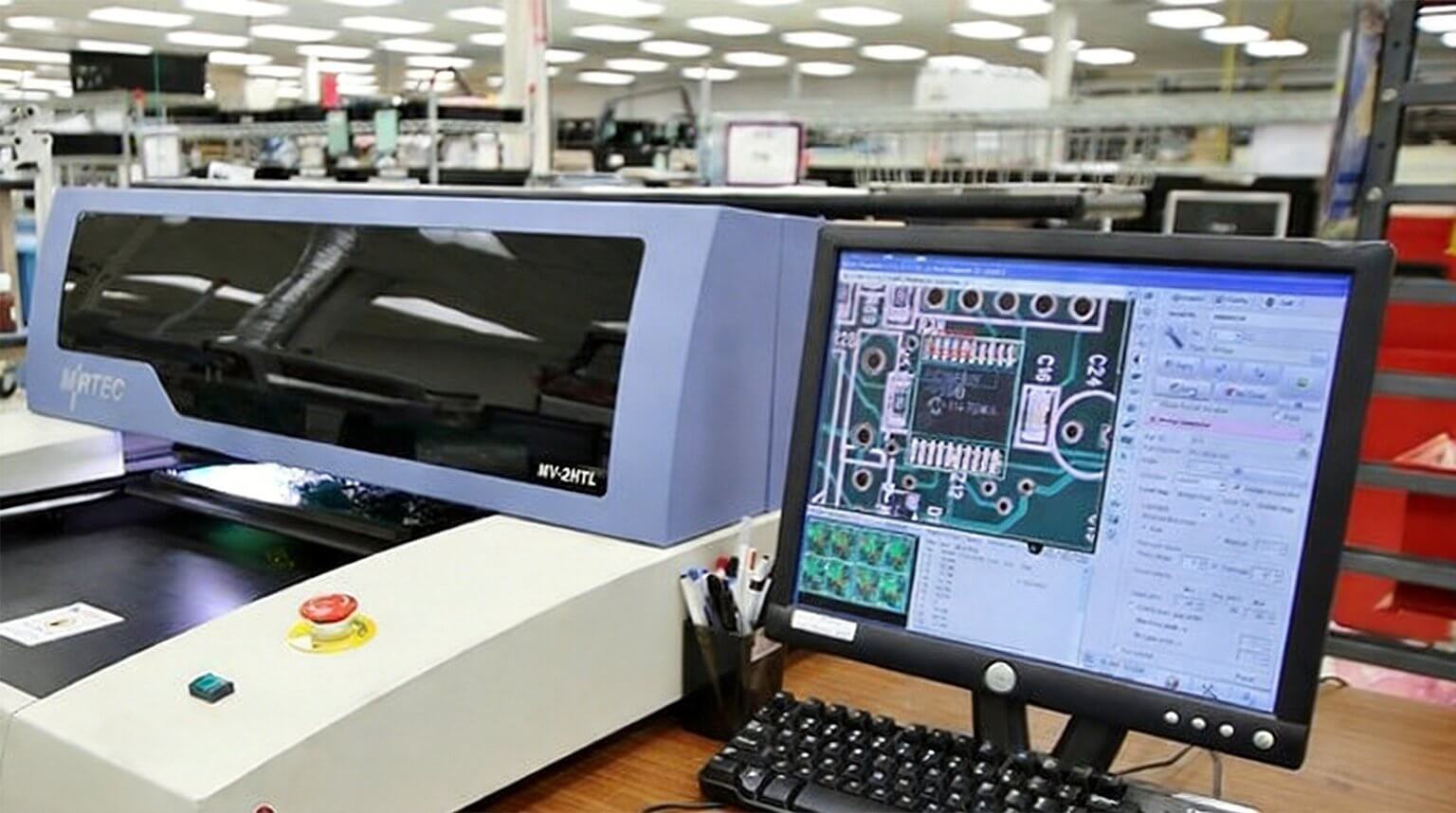
What Is AOI Inspection in PCB
AOI, or Automated Optical Inspection, is a key inspection method in PCB manufacturing. In this article, we explain what AOI is, how it works, and why it matters in PCB fabrication and assembly.
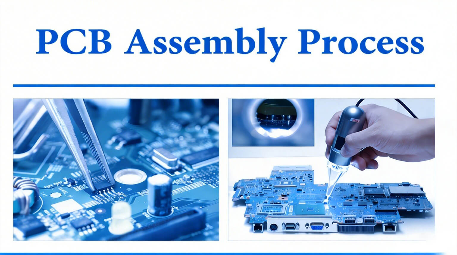
SMT PCB Assembly Process Explained
Learn the complete SMT PCB assembly process flow, from solder paste printing and component placement to reflow soldering and X-ray inspection. Step-by-step guide for reliable PCB manufacturing.
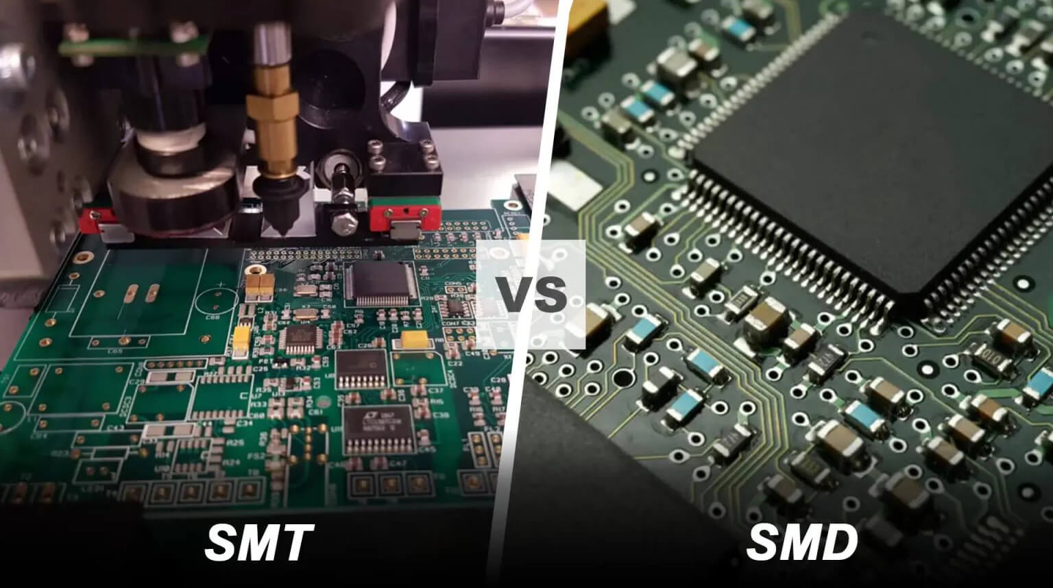
What Is the Difference Between SMT and SMD
Learn the difference between SMT and SMD in PCB assembly. A beginner-friendly guide explaining definitions, key differences, and how they work together in electronics manufacturing.

Everything You Need to Know About PCB Files
Learn what PCB files are, which formats are required for fabrication and assembly, and how to generate Gerber, BOM, and pick-and-place files correctly.

What Is a PCB BOM File
Discover the essentials of PCB BOM files in this beginner’s guide. Learn about their role in PCB design, how to create accurate BOMs, and best practices for engineers and designers.

Design for Assembly (DFA) Guide for Successful PCBA Projects
Master DFA for PCBA projects with our complete guide: from component placement, pad design, thermal management, test points, to pre-production checklists for error-free assembly.

A Practical Guide to Prevent PCB BOM Errors Before Assembly
Learn how to prevent PCB BOM errors before assembly. This practical guide explains EMS-ready BOM formats, alternates, DNP handling, and real-world SMT pitfalls.
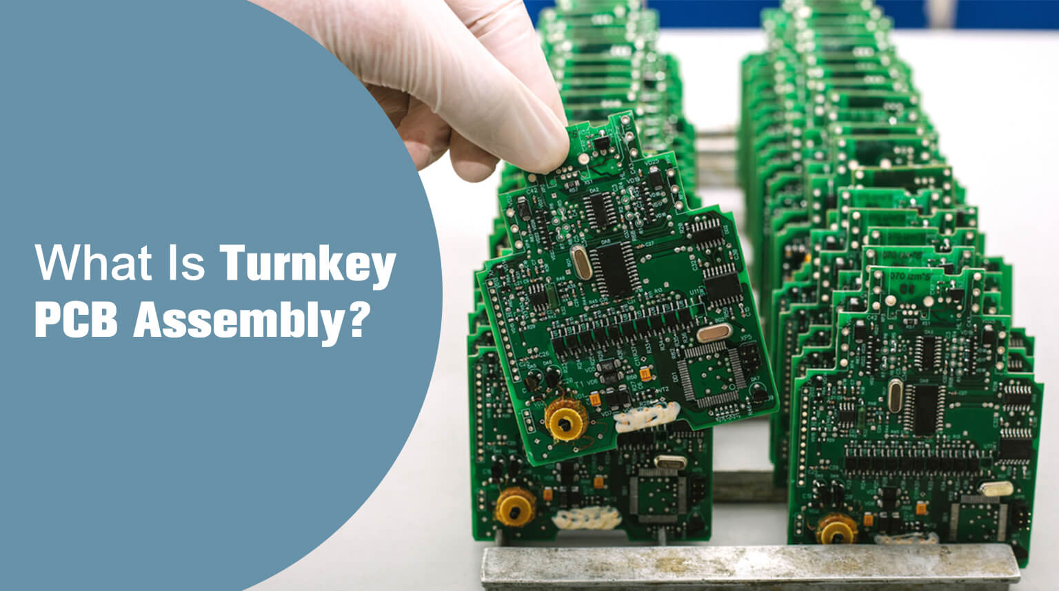
What Is Turnkey PCB Assembly?
Turnkey PCB assembly is a one-stop PCBA solution covering PCB fabrication, component sourcing, assembly, and testing. This article explains what it is, key types, benefits, and how to choose the right provider.

Should You Outsource PCB Assembly? Pros & Risks
Outsourcing PCB assembly can reduce costs, speed time-to-market, and add flexibility—but it also carries risks. This guide explains the differences, pros, risks, and how to decide.

What’s the Difference Between PCB and PCBA?
PCB is the bare circuit board. PCBA is the fully assembled, working board. This guide explains their real differences, why it matters, and how choosing wrong can cost you time and money.
