banner下面提交表单 (#30)

HDI Solutions for High-Performance Electronics

As electronic products become smaller, faster, and more powerful, HDI technology has become essential for modern product design. It helps increase component density, reduce board size, and improve signal integrity in compact electronic systems.

With 20+ years of electronics manufacturing experience and 5,200+ completed projects, PCBCool supports customers from HDI PCB fabrication to PCBA and box-build assembly, helping turn advanced HDI designs into reliable, production-ready electronic products.

Proven Technology

Microvias, blind/buried vias, stacked/staggered vias, resin plug vias, via-in-pad, impedance control.

Qualified Materials

Shengyi, Rogers, Panasonic, Isola, Ventec, ITEQ, DuPont, Taconic, and customer-specified laminates.

Advanced Features

Edge plating, gold fingers, half holes, countersink holes, press-fit holes, carbon ink, peelable mask.

Engineering Support

Stack-up review, DFM feedback, impedance planning, material selection, and risk evaluation.

What Makes HDI PCB Projects Difficult

HDI PCB manufacturing is not difficult simply because the board is smaller. For manufacturers, the real challenge is that several high-risk processes must be controlled together within a very limited margin for error.

01

Microvia Control

Laser drilling, copper plating, via filling, and stacked via connection must stay consistent inside a very small vertical structure.

02

Fine Trace Control

Fine traces and tight spacing require stable line width, spacing, copper thickness, and solder mask alignment across the full panel.

03

Layer Alignment

After each sequential lamination step, buried vias, laser microvias, inner layers, and outer patterns must remain accurately aligned.

04

Stack-Up Control

Dielectric thickness, copper weight, material behavior, trace geometry, and return paths must match the real manufacturing process.

05

PCBA Readiness

BGA, via-in-pad, surface finish, flatness, solderability, and testing access must be considered before PCBA.

Early Engineering Review for HDI Projects

Because these HDI manufacturing challenges are closely connected, PCBCool’s engineering team gets involved before production begins.

Once you send us your Gerber files, BOM, stack-up, and project requirements, our engineers will review the key manufacturing details, discuss any concerns with you, and confirm a clear production plan before moving forward.

Practical Review Path

Submit Project Files

Gerber files, BOM, stack-up, and basic project requirements.

Manufacturability Review

Review key HDI risks before fabrication and assembly.

HDI PCB to PCBA Plan

Recommend a practical path from HDI fabrication to PCBA production.

HDI PCB Technical Capabilities

PCBCool supports HDI PCB manufacturing based on IPC Class 2 and Class 3 requirements. The specifications below help customers evaluate our manufacturing capabilities for complex HDI PCB projects.

Capability Categories
Detailed Specifications
HDI Structure
8 Items
Layer Count
1–40 Layers
HDI Build-Up
1+N+1, 2+N+2, 3+N+3, 4+N+4, Any-Layer HDI
Board Thickness
0.037 mm – 6.5 mm
Board Dimension
1–2 Layers: 1500 × 600 mm; Multilayer: 620 × 720 mm
Minimum Laser Microvia
0.08 mm
Minimum Mechanical Drill
0.15 mm
Aspect Ratio
Standard 25:1; Max. 35:1
Blind Via Aspect Ratio
0.8:1
Detailed Specifications
Materials
6 Items
Base Materials
FR4, Halogen-Free, Metal Core, Polyimide, High-Frequency Materials, Mixed Lamination
FR4 Tg Options
Tg 140, Tg 170, Tg 180
High-Frequency Materials
Rogers 4350B, 3003, 4003C, 5880; Taconic; Teflon
Material Brands
KB, ITEQ, Shengyi, Isola, Rogers, Ventec, Panasonic, Taconic, Nelco, Bergquist, DENKA, or customer-specified laminates
Flammability
UL 94V-0
Thermal Conductivity
0.3–400 W/m·K, depending on material type
Detailed Specifications
Fine Line & Registration
8 Items
Minimum Trace / Space
64 μm / 64 μm
Line Width / Space Tolerance
±0.015 mm
Minimum Annular Ring
50 μm
Minimum Pad-to-Pad Clearance
40 μm
Layer-to-Layer Registration
≤100 μm
Solder Mask Registration
≤38 μm
Minimum Solder Mask Clearance
2 mil
Solder Mask Dam
50 μm
Detailed Specifications
Copper & Finish
6 Items
Copper Thickness
1/3 oz – 33 oz
Surface Finishes
HASL Lead-Free, ENIG, OSP, Immersion Silver, Immersion Tin, Hard Gold, Gold Fingers, Carbon Ink, Bare Copper
Solder Mask Colors
Green, White, Black, Blue, Red, Yellow, Orange, Purple, Matte Green, Matte Black
Solder Mask Brands
RongDa, KuangShun, Coants, LanBang, Taiyo
Solder Mask Thickness
0.2 mil – 1.6 mil
Via Plugging
0.2 mm – 0.8 mm
Detailed Specifications
Tolerance & Testing
10 Items
Board Thickness Tolerance
±5%
Hole Diameter Tolerance
±0.05 mm
Hole Location Tolerance
±2 mil
Outline Tolerance
±0.1 mm
V-Cut Tolerance
±10 mil
Beveled Edge Tolerance
±5 mil
Impedance Tolerance
50Ω, ±10%
Warp and Twist
≤0.50%
Quality Standards
IPC Class 2 / Class 3
Quality Testing
AOI, 100% Electrical Test
Detailed Specifications
Advanced Processes
7 Items
Advanced Via Processes
Blind Vias, Buried Vias, Laser Microvias, Via-in-Pad, Resin Plugged Vias
Mechanical Features
Castellated Holes, Press-Fit Holes, Countersink / Counterbore Holes, Edge Plating
Special PCB Processes
Thick Copper, Copper Block Embedded, Z-Axis Milling, Gold Fingers, Carbon Ink, Peelable Solder Mask
High-Frequency Support
High-Frequency Materials, High-Frequency Mixed Lamination, Foam Board
Engineering Services
DFM Check, Stack-Up Review, Impedance Review
Expedited Production
24-Hour Expedited Production Available
Data Formats
Gerber, DXF, PCBdoc, ODB++, HPGL, BRD

End-to-End Solutions

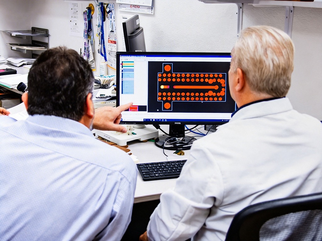
Two designers are discussing the HDI PCB design submitted by the client

With 177 engineering and R&D personnel and a turnkey EMS manufacturing system, PCBCool can provide flexible support for different stages of HDI projects.

  • Answer Engineering Support
  • Answer PCB Fabrication
  • Answer PCBA Assembly
  • Answer Box Build / System Integration
  • Answer Testing & Validation
  • Answer Supply Chain & Logistics
Two designers are discussing the HDI PCB design submitted by the client
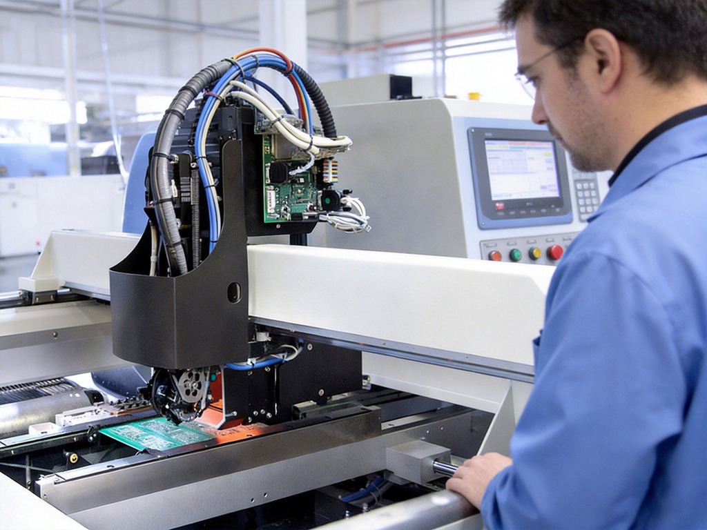
A worker is waiting for HDI PCB assembly

Advanced Technologies

A worker is waiting for HDI PCB assembly

On the manufacturing side, PCBCool is equipped with advanced equipment such as vacuum etching and laser drilling, supporting fine traces, microvias, and multi-step build-up structures.

  • Answer Vacuum etching supports 64 μm / 64 μm minimum trace/space
  • Answer Laser drilling supports 0.08 mm minimum microvias
  • Answer Fast HDI PCB prototyping in as little as 10 days
  • Answer Supports 1+N+1 to 4+N+4 and any-layer HDI build-up structures
  • Answer Supports SBU technology for complex multi-step HDI projects
  • Answer PCB 220k m²/month with PCBA 15M SMT points/day
HDI PCB Project Showcase

Explore how PCBCool supports customer HDI projects through selected case examples and HDI PCB / PCBA samples from past production.

01
Build-Up Feasibility

HDI Designs That Need a Practical Build Route

When routing density exceeds standard multilayer PCB limits, customers need to confirm whether the chosen HDI build-up can be manufactured without unnecessary lamination steps, yield loss, or cost escalation.

Build-Up Route Layer Planning Cost Control
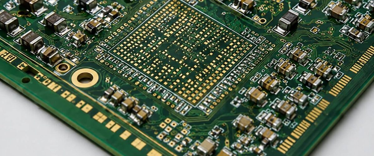
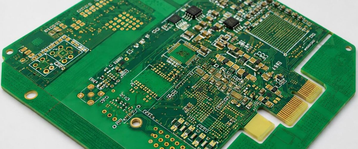
HDI PCB functional main board sample with dense routing and gold plated pads
02
HDI Build Control

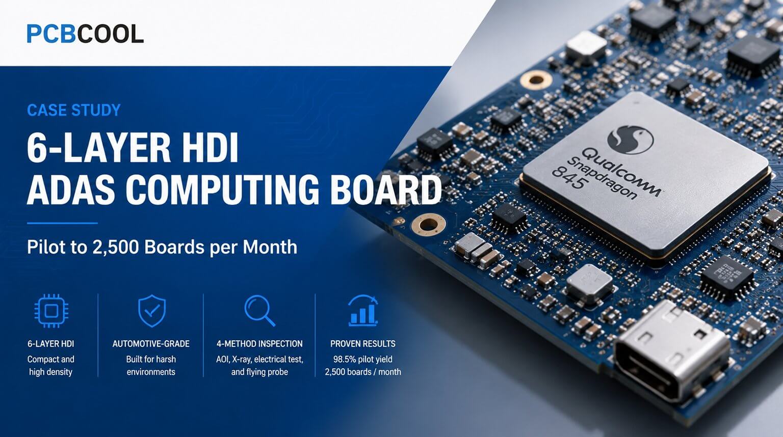
A 6-Layer HDI Stackup Built for Stable Yield

The 6-layer HDI structure was built to keep microvia, lamination, and ENIG processes stable from pilot validation to monthly production.

6-Layer HDI Sequential Lamination ENIG
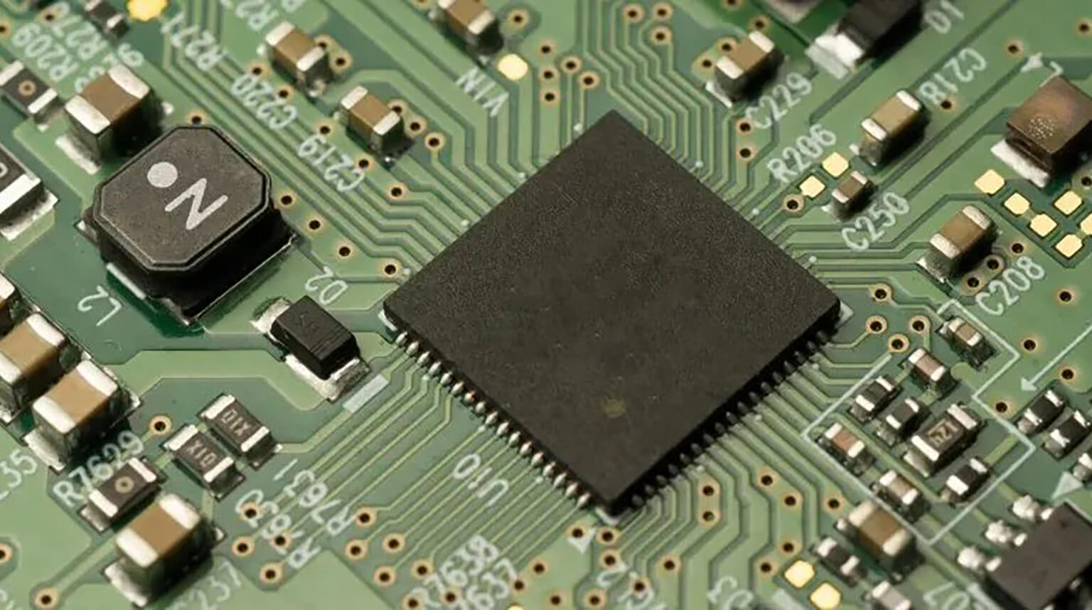
6 layer HDI PCB stackup with laser drilled microvias and ENIG finish
03
BGA-Driven HDI

HDI PCB Projects for Fine-Pitch BGA Devices

When a product uses fine-pitch BGA devices, the PCB must support dense fanout routing, compact component placement, and a reliable transition from layout to assembly.

Fine-Pitch BGA Fanout Routing PCB to PCBA
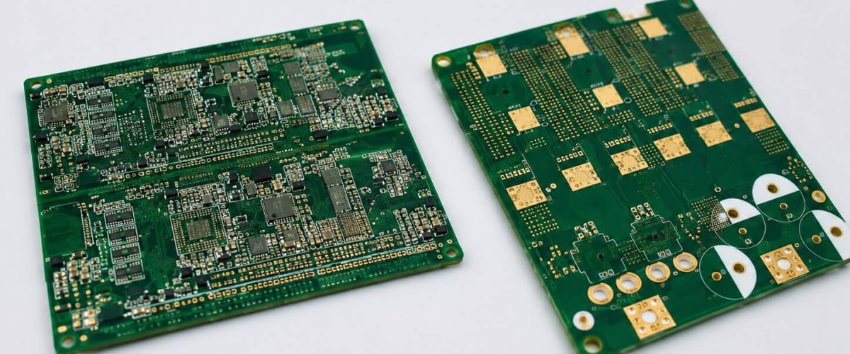
HDI PCB and PCBA sample boards for compact electronic manufacturing projects

Commitment to Quality

An upward pointing arrow icon

Certification Compliance Support

  • Answer Support for ISO 9001 quality management system
  • Answer Compliance with ISO 14001 environmental management system
  • Answer Adherence to ISO 45001 occupational health and safety standards
  • Answer Compliance with IPC-A-610 and IPC J-STD-001 standards
  • Answer Support for RoHS / REACH environmental compliance
  • Answer Support for UL and CE certifications
  • Answer Support for ISO 13485, IEC 62031, and other industry-specific certifications

An icon for controlling the screen

Manufacturing Process Control

  • Answer Full BOM and lot traceability across production
  • Answer Material traceability (components, boards, solder paste, etc.)
  • Answer Process documentation for regulated manufacturing
  • Answer First Article Inspection (FAI) support
  • Answer In-process quality checks and monitoring
  • Answer Controlled ESD & cleanroom processes (if applicable)
  • Answer Complete inspection records and test reports
  • Answer Change control and nonconformance management

More Advanced PCB Solutions

Complex Stack-Up

Multilayer PCB

For products that need more routing space, stable layer alignment, and reliable multilayer fabrication.

Low-Loss Materials

High-Frequency PCB

For RF, microwave, and communication products that require stable signal transmission and suitable laminate selection.

Space-Saving Design

Rigid-Flex PCB

For compact products that need flexible connections, fewer connectors, and better use of internal space.

Signal Performance

Controlled Impedance PCB

For designs where stack-up, materials, and manufacturing tolerance must support stable electrical performance.

BGA Fanout

Via-in-Pad PCB

For dense HDI layouts where routing space is limited and vias need to be placed directly in pads.

Fine-Pitch SMT

BGA Assembly

For HDI projects that use fine-pitch BGA packages and require careful assembly preparation.

Ready to Move Your Project Forward?

Send us your project details. PCBCool will help review the technical requirements and recommend a suitable PCB manufacturing approach.

Frequently Asked Questions

Q1: Can PCBCool Be Involved in the Project from the Design Stage?

A: Yes, we have an R&D department that can handle everything from 0 to 1 design, design upgrades, and optimizations.

Q2: Does PCBCool Offer Design File Review Services?

A: Yes, we review all design files to ensure they meet manufacturing requirements, which is part of our quality control process.

Q3: How Does PCBCool Support HDI PCB Design Issues?

A: When we identify an issue, we will immediately contact you and organize a meeting, either on-site or online, where our engineering team and business manager will work with you to find a solution.

Q4: Can PCBCool Serve the Military Industry?

A: Yes, we have extensive experience in providing services to industries such as military, communications, automotive, medical, consumer electronics, aerospace, and more.

Q5: What Is the Lead Time for HDI PCB Projects?

A: For complex HDI PCB projects, the manufacturing and assembly process typically takes 15-30 working days. We also offer expedited services for urgent needs.

Q6: How Can I Get a Quote for My HDI PCB Project from PCBCool?

A: You need to provide your design files and project specifications. After review, our team will provide you with a detailed quote and lead time.

Q7: Does PCBCool Offer Long-Term Supply Support for HDI PCB?

A: Yes, we are committed to providing long-term B2B EMS services and building strategic, long-term partnerships with our clients.

Q8: Does PCBCool Work with Startups?

A: Yes, we have experience working with startups and helping them grow as their business develops.

Q9: Can PCBCool Assist with Component Procurement?

A: Yes, our turnkey service includes component procurement. We source components from reliable manufacturers or authorized distributors to ensure product authenticity.

Q10: Does PCBCool Support Mixed-Component Assembly for HDI PCB?

A: Yes, we have SMT, THT, and manual assembly lines that can handle both fine-pitch components and large-pin components for mixed-technology assembly.

Q11: Does HDI PCB Assembly Require Special Soldering Techniques?

A: No, HDI PCB assembly uses traditional reflow and wave soldering techniques, but it requires more precise temperature and process control to ensure high-quality soldering.

Q12: Does PCBCool Provide After-Sales Support?

A: Absolutely. We assign a dedicated account manager to every customer, responsible for handling everything from pre-sale to after-sale, ensuring any issues are promptly addressed.

HDI PCB Technical Insights