Designing a printed circuit board (PCB) is often the stage where new designers focus heavily on component placement and signal routing, while paying far less attention to the small yet critical details of the manufacturing process. The annular ring is one of those overlooked details that can ultimately determine whether a PCB is successfully manufactured—or rejected during fabrication.
This tutorial is written specifically for beginners and junior PCB designers. By the end of this article, you will understand how to design a 1–4 layer PCB that not only meets standard manufacturing requirements, but also performs reliably in real production environments, rather than failing at the fabrication stage.
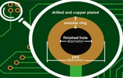
In simple terms, an annular ring is the remaining copper pad around a hole after drilling.
During PCB fabrication, holes are first drilled mechanically and then copper-plated. While the plated hole wall provides vertical electrical connectivity, the annular ring provides the critical copper land that ensures a reliable electrical and mechanical connection to the surrounding traces or planes.
These holes are typically used for:
- Through-hole components
- Vias connecting PCB layers
- Mounting or mechanical holes
Without sufficient annular ring width, this connection becomes weak and prone to defects such as:
- Pad breakout
- Poor plating adhesion
- Open circuits
Annular rings appear on any copper layer where a pad is defined. On single- and double-sided PCBs, they exist on the top and bottom layers. In multi-layer boards, annular rings also appear on inner copper layers.
In PCB fabrication, holes are rarely drilled perfectly at the center of a pad. Slight deviations can occur due to mechanical vibration, material movement, or tool wear. This unavoidable variation is commonly referred to as drill tolerance or drill wander.
When the annular ring is too small, the drilled hole may partially cut into the copper pad or, in severe cases, remove the pad entirely. This condition, often called pad breakout, can lead to immediate fabrication failure.
A properly sized annular ring ensures:
- Strong and consistent solder joints for through-hole components
- Reliable electrical interconnections between PCB layers
- Improved mechanical strength for connectors and terminal blocks
- Long-term reliability under vibration and thermal stress
In practice, many PCB rejections occur not because of complex circuit errors, but due to basic fabrication rule violations, with insufficient annular ring sizing being one of the most common. Designing with safe annular ring values significantly increases the likelihood of first-pass manufacturing success.
Understanding the locations of annular rings on a PCB is essential when deciding their sizes during the design phase. Following these guidelines helps avoid manufacturing issues and costly redesigns, even for first-time PCB designers.
Components such as resistors, capacitors, connectors, relays, inductive components, and terminal blocks are mounted on through-hole pads. These components experience mechanical stress during insertion and soldering, especially during hand assembly. For this reason, through-hole pads should have larger annular rings to ensure mechanical durability and reliable solder joints.
Recommended Annular Ring Sizes:
- Minimum Annular Ring: 0.25 mm
- Recommended Annular Ring: 0.3–0.4 mm
Example:
- Drill Size: 0.8 mm
- Pad Size: 1.4–1.6 mm
These values provide a sufficient margin for drill tolerance while ensuring strong and reliable solder joints.
Vias interconnect layers in multi-layer PCBs. Although via annular rings are generally smaller than component pads, they are still crucial for electrical reliability. Poorly sized via annular rings can lead to intermittent connections, open circuits, or failures under repeated thermal cycling.
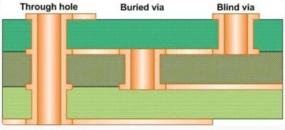
The main types of vias are:
- Through-Hole: passes through all layers
- Buried Via: connects inner layers only
- Blind Via: connects outer layer to one or more inner layers
Recommended Via Sizes (1–4 Layer Boards):
- Minimum Annular Ring: 0.15 mm
- Recommended Annular Ring: 0.2 mm
Example:
- Via Drill: 0.3 mm
- Via Pad: 0.7 mm
These via sizes are compatible with most PCB fabricators and suitable for high-speed signals or moderate current-carrying vias.
Mounting holes are used for screws, standoffs, or other mechanical fixtures. These holes can be either isolated or grounded. When grounded, they must have sufficiently large annular rings to maintain a solid copper connection, ensuring both mechanical stability and electrical continuity.
This section provides practical steps you can apply in any PCB design software, such as Altium Designer, KiCad, or EasyEDA.
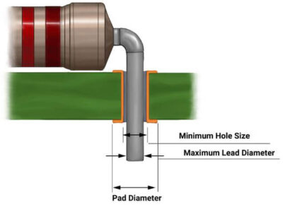
Start by checking the component datasheet for lead diameter.
Always add clearance to account for copper plating and manufacturing tolerance.
Example:
- Component Lead Diameter: 0.6 mm
- Final Drill Size: 0.8 mm
This small clearance ensures smooth component insertion and reliable soldering.
To calculate pad diameter, use this formula:
Pad Diameter = Drill Diameter + (2 × Annular Ring)
Example:
- Drill: 0.8 mm
- Annular Ring: 0.3 mm
- Pad Diameter: 1.4 mm
This ensures that even after a misaligned drill, enough copper remains around the hole to maintain mechanical and electrical integrity.
Design rules act as automatic safeguards against mistakes. Beginners should always define these rules before routing the board:
- Minimum annular ring
- Minimum via diameter
- Minimum drill size
Recommended Values:
- Via drill ≥ 0.3 mm
- Via pad ≥ 0.7 mm
- Annular ring ≥ 0.2 mm
Once these rules are set, the software will automatically detect violations, preventing fabrication issues.
- To avoid weak connections, keep vias away from pad edges.
- For power and ground connections, use larger vias for better mechanical and electrical performance.
- Do not place vias where no pad exists or under the solder mask.
- Increasing via size can also improve current flow and thermal performance.
- Mistake 1: Using Pads That Are Too Small
Always calculate the annular rings instead of guessing pad sizes.
- Mistake 2: Using Small Vias
Small vias may look neat, but they can exceed manufacturer limits or cause fabrication problems.
- Mistake 3: Ignoring Manufacturer’s Fabrication Guidelines
Review the manufacturer’s minimum drill and annular ring specifications.
- Mistake 4: Omitting Teardrops
Always add teardrops where tracks meet pads, especially for high-stress connections.
Before generating the Gerber files, ensure:
- Annular rings are visible on all pads.
- No drill holes cut into pad edges.
- All layers have proper via connections.
- DRC (Design Rule Check) passes without errors.
- Manufacturer limits are respected.
Following these checks can prevent costly mistakes and improve first-pass manufacturing success.
Annular rings might seem like minor PCB elements, but they have a major impact on both manufacturing success and long-term reliability. Even beginners can produce high-quality multi-layer PCBs by using the correct drill sizes, calculating the proper pad sizes, and applying sound design principles.
By following the practical steps in this tutorial, your PCB designs will be easier to manufacture, more reliable in operation, and more likely to pass fabrication checks.
For engineers and designers looking for a comprehensive set of PCB design resources, tools, and guidelines, PCBCool provides everything you need to streamline your PCB design process and ensure your designs meet industry standards. Whether it’s DFM tips, annular ring calculators, or design rule templates, PCBCool helps you take your PCB projects from prototype to production with confidence.