Any-layer PCB design is not “high tech for no reason.” It exists because parts got smaller and boards got tighter. Ten or fifteen years ago, you could route most boards with normal through-hole vias and 2-4 layers. Even when BGA showed up, the pitch was often big enough that dog-bone fanout still worked.
Now the common stuff is harder: tight BGA, small QFN, fast memory, fast clocks, and boards that must fit inside tiny housings. You try the usual routing tricks, and you hit a wall. The drill is too big, the pads are too close, the traces have no room, and your nice solid ground plane ends up full of holes.
Any-layer PCB fixes one big problem: they let you change layers almost anywhere, not just on the outer layers or in a few special spots. That sounds simple, but it changes the whole routing game. When you can drop a signal down one layer right under the part, you don’t need to push long traces across the board just to find a “legal” via.
People also call this technology ELIC (every-layer interconnect). The idea is the same: microvias can be used between every pair of adjacent layers.
This article explains any-layer PCB in plain words. No marketing. No theory-heavy talk. Just what it is, how it’s built, how you design it, what you must ask your manufacturer, and how you avoid expensive mistakes.
A normal multilayer PCB uses a mix of via types:
- Durchsteckbohrung drilled all the way through the board.
- Blindbohrung goes from the top layer down to an inner layer, but not through the whole board.
- Begrabene Via: stays inside the board and doesn’t reach the outer surfaces.
Those options work fine for many designs, but they also put limits on you. The big issue is that normal drill vias are big, and they take up space on every layer they pass through. On dense boards, that kills routing space fast.
An any-layer PCB uses laser microvias between any adjacent layers. That means:
- Layer 1 <-> Layer 2 microvias are allowed
- Layer 2 <-> Layer 3 microvias are allowed
- Layer 3 <-> Layer 4 microvias are allowed
- …and so on through the whole stack
So you can “step” signals down through the board like stairs. Instead of using one big via that punches through everything, you use a chain of small microvias.
That single change gives you two big benefits:
- You don’t block inner layers with huge via pads.
- You can escape dense parts cleanly without ugly long detours.
“Any-layer” does not mean you stop planning. It just means you have more options.
On a standard board, a designer often routes like this:
- Try to route on top
- When stuck, drop through a via
- But the via might block a plane or a channel
- So you reroute and compromise
- You end up with long, messy traces
On any-layer board, you can do this instead:
- Place the part
- Decide where each signal should escape
- Drop it down right there
- Route away on the next layer
It becomes less of a fight.
A good way to think about it: any-layer is mostly a “BGA escape” technology. That is the moment where routing gets impossible on a normal stackup.
Any-layer boards are built in steps. The key process is sequential lamination. The manufacturer:
- Laminate some layers
- Laser drills microvias
- Plates the microvias
- Laminates more layers
- Repeats until the full stack is built
This matters to you as a designer because:
- Every extra lamination step costs money
- Every step adds alignment risk
- Some via structures are harder to plate reliably
That is why any-layer PCB are expensive. You are paying for extra process steps, not magic materials.
If you do not need any-layer, do not use it. That is the blunt truth.
Any-layer is usually chosen because at least one of these is true:
- BGA pitch is very tight (0.5 mm, 0.4 mm, or smaller)
- Board size is fixed and cannot grow
- The design needs very short signal paths (high-speed buses, RF sections)
- You must keep layers clean (planes can’t be destroyed by through-holes)
If the board is not that dense, a simpler HDI stack (like 1+N+1) might be enough. It can be much cheaper and faster.
Also, your lead time grows because the factory has more steps, more inspection, and more chances for rework.
Microvias are tiny laser-drilled vias. Common numbers vary by manufacturer, but the concept stays the same:
- They are small
- They are shallow
- They must be plated well
Depth vs Diameter Rule
Microvias have a key limit: they cannot be too deep compared to their diameter. If the via is too deep, plating becomes unreliable. That is how you get weak vias that crack later.
Most factories follow a simple rule (rule of thumb): keep microvias close to a 1:1 depth-to-hole ratio.
So as a designer, you do not guess this. You do this instead:
- Ask your PCB house for their any-layer stackup
- Ask for their standard microvia drill size
- Ask for the dielectric thickness between adjacent layers
- Build your design rules around that
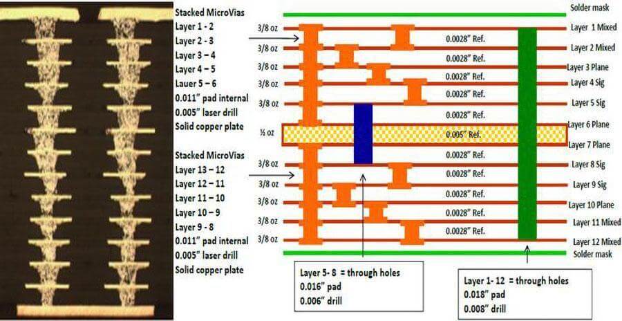
There are two common ways to chain microvias through layers:
- Stacked Microvias: A microvia sits directly on top of another microvia. It saves space, but it can be more fragile and more expensive because it often needs filling and careful plating.
- Staggered Microvias: The microvias are offset like a staircase. It uses a bit more area but is usually more forgiving.
If this is your first any-layer board, staggered is the safer choice unless your manufacturer specifically says stacked is fine and you can afford the cost.
Here is a simple workflow that keeps you out of trouble:
Don’t design first and ask later. Ask the manufacturer first. Get:
- Schichtanzahl
- Dielectric thickness between layers
- Copper weights
- Microvia drill and pad capability
- Whether they support via-fill and via-cap
A common clean setup:
- One or more layers are solid ground
- One or more layers are power (or split power islands if needed)
- Remaining layers carry signals
- Even if you have many layers, don’t make every layer “random routing.” It becomes hard to debug and easy to break return paths.
Don’t start routing the easiest pins first. Plan the escape like a map:
- Which rows stay on top?
- Which rows drop to Layer 2?
- Which ones drop deeper?
- Which nets must stay short? (clocks, DDR, RF)
- If you skip this planning, you will reroute 3 times later.
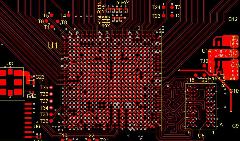
A basic BGA escape approach that works well:
- Outer Row: route on Layer 1
- Second Row: microvia in pad -> Layer 2 route
- Inner Row: microvia to a deeper layer (using a chain)
You keep traces short, and you avoid big via pads blocking everything.
If you place a via inside a BGA pad and leave it open, solder can wick down the hole during reflow. That creates weak joints, uneven solder, or openings.
That is why many any-layer designs use VIPPO (via-in-pad plated over):
- Drill the via in the pad
- Plate it
- Fill it
- Cap/plate over it so the pad is flat again
You must call this out in fab notes if you want it. Do not assume it is included.
Any-layer boards can still fail badly if you destroy your reference planes.
High-speed signals need a solid return path, usually a ground plane. If you cut the plane with too many antipads or via fences, the return current has to detour. That increases noise and EMI.
Two Easy Rules:
- Keep at least one ground layer as continuous as possible.
- When a signal changes layers, give it a nearby ground via so the return path can also change layers.
Any-layer boards often need clearer documentation than a normal PCB.
Drill/Via Info
Your factory needs to clearly understand:
- Which holes are microvias (laser)
- Which holes are mechanical
- Which vias are filled and capped
- Which are normal plated holes
Notes to Add in Fab Drawing
- Laser microvias between adjacent layers: L1-L2, L2-L3, …
- Via-in-pad: filled and plated over (VIPPO) on BGA pads
- Controlled impedance on nets: ___ ohm single-ended / ___ ohm diff (if needed)
- Stackup per manufacturer standard any-layer build
- IPC class requirement (if you have one)
Even if you use a fab house that “knows,” do not leave it vague. Vague notes cause wrong quotes, delays, or wrong builds.
- Problem 1: Microvia Cracking
Causes:
Often caused by aggressive stacked vias, bad aspect ratio, or harsh thermal cycling.
Prevention:
Follow the manufacturer’s microvia limits, prefer staggered, don’t push minimums for no reason.
- Problem 2: Solder Wicking
Causes:
Happens when the via-in-pad is open.
Prevention:
VIPPO callout.
- Problem 3: Misregistration
Causes:
Layers don’t line up perfectly during lamination.
Prevention:
Keep microvia pads with enough land, avoid ultra-tiny rings, and follow fab tolerances.
- Problem 4: Ground Plane “Swiss Cheese”
Causes:
Too many antipads and voids.
Prevention:
Keep via clusters tight, don’t slice planes with long rows, stitch grounds.
Worth It:
- Very dense BGA
- Small consumer devices
- High-speed memory buses
- RF + digital mixed boards where layout control is critical
- Boards that must be small (and enclosure cost is high)
Not Worth It:
- Slow digital, low pin count
- Large boards with plenty of area
- Cost-sensitive products
- Designs that route fine with 1+N+1 HDI or even standard multilayer
A simple decision trick: If you can solve the routing problem by adding an area or changing a package, do that first. Any-layer should be the last option, not the first.
Before you send files out:
- Stackup confirmed with manufacturer
- Microvia sizes confirmed
- Aspect ratio respected
- VIPPO clearly noted (if used)
- Ground planes checked for splits / bottlenecks
- Layer transitions have nearby ground vias
- Separate drill files or clear via definitions
- BGA fanout reviewed (no blocked channels)
- DRC clean (especially via-to-via clearance and pad-to-pad clearance)
This checklist saves you from the most common “first any-layer” mistakes.
Any-layer PCB design is not magic. It is a practical solution for modern routing problems. It gives you freedom to move signals between layers right where you need them. That freedom can turn an impossible BGA into a routable design.
But you pay for it with cost, lead time, and tighter manufacturing rules. That is why a good any-layer design is mostly about planning:
- Lock the stackup early
- Use microvias correctly
- Choose stacked vs staggered wisely
- Plan BGA escape before routing
- Keep at least one ground plane strong
- Document via types and VIPPO clearly
If you do those things, any-layer becomes manageable. It stops being scary and becomes just another tool in your PCB toolbox.