The importance of PCB design is a fundamental skill for electronics engineers. Whether you’re working on embedded systems, power electronics, IoT devices, or communication circuits, the ability to design a well-structured PCB is key to successful product development.
Although most students are familiar with circuit theory, many struggle to translate a schematic diagram into a practical PCB layout. This gap in skills often presents a significant challenge, especially when trying to move from theory to actual product design. To bridge this gap, CAD software plays a crucial role in helping engineers visualize and create the physical layout of their circuits.
Among the many PCB design tools available, Altium Designer stands out for its comprehensive capabilities, offering integrated schematic capture, PCB layout, design rule checks, and manufacturing output generation. However, its wide range of features can overwhelm beginners, as the software’s interface is packed with numerous options and settings that may seem intimidating at first.
In this tutorial, we will walk you through the entire PCB design process using Altium Designer. Starting from the initial concept, we’ll guide you through creating a fully functional Mehrlagen-Leiterplatte, ready for manufacturing.
Every PCB design in Altium begins with a project, which acts as a container for all related files—schematics, PCB layouts, libraries, and output files. By organizing these elements within a single project, it becomes much easier to manage the design and ensure you never lose track of your documents in the future.
To start a new PCB project in Altium Designer, follow these steps:
- Launch software. A blank workspace will open.
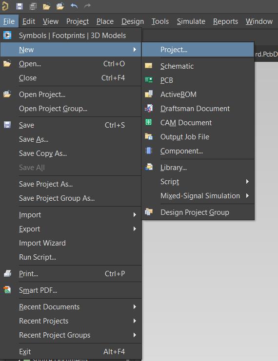
- In the top-right corner, click on File.
- Select File > New > Project.
- In the display panel, click on Project and assign a proper name to your project.
- Choose the folder where you’d like to save your project.
- Save the project file with a .PrjPcb extension.
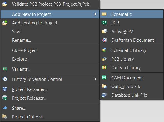
Once the project is created, the next step is to add the necessary design files: a schematic sheet and a PCB layout. The schematic document holds the circuit diagram with components and their associated footprints, while the PCB document defines the physical layout and electrical connections of your board. To add these documents to the project, follow these steps:
- Right-click on the PCB project in the Project panel.
- Select Add New to Project > Schematic to add a blank schematic sheet.
- Repeat the process and select Add New to Project > PCB to add the PCB layout file.
- Name your schematic and PCB files, and save them using Ctrl + S.
To draw a circuit, you will need various components, such as resistors, capacitors, inductors, integrated circuits (ICs), connectors, regulators, and many others. In Altium Designer, components are divided into two primary categories: schematic symbols and PCB footprints. Schematic symbols are used to represent components in the circuit diagram, while PCB footprints define the physical layout.
Altium Designer comes with built-in libraries, which contain verified component symbols and footprints. These general-purpose libraries are ideal for beginners, providing a wide range of commonly used components. However, they may not include some advanced or specialized components. For this reason, it is valuable for beginners to learn how to create custom footprints manually for components that are not available in the standard libraries.
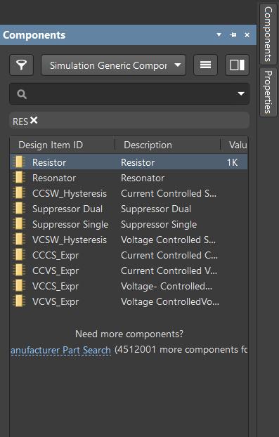
To add components to your schematic sheet, follow these steps:
- On the left panel of the schematic sheet, you will find the Components option at the top left.
- Click on Components to open the general-purpose library.
- Use the search function to find the desired component, such as resistors, capacitors, and more.
- Double-click on the component you wish to use, and it will be added to your schematic sheet.
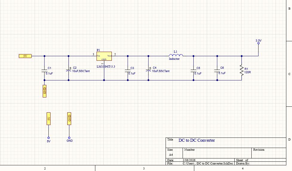
The schematic is a visual representation of the circuit, showing how components are connected and how the electrical signals flow between them. A well-organized and professional schematic minimizes errors and streamlines the debugging process, saving valuable time.
When placing components, follow a logical layout. A simple approach is to place inputs on the left, outputs on the right, with the power circuit at the top and ground at the bottom. This flow creates a clean, easy-to-follow schematic that is more efficient to work with.
While designing your circuit, avoid crossing wires and keep the connections neat. Instead of using long wires to connect distant components, use net labels to indicate connections between far-apart signals.
After completing the schematic, it’s crucial to compile the project to check for errors. Look for issues like unconnected nets or redundant names. A schematic with a logical flow and correct connections will make the next steps in the design process, including PCB layout, much smoother.
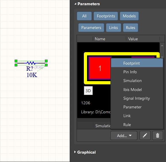
Each component in your schematic requires a corresponding physical footprint, which defines the size and shape of the PCB pads. For example, resistors and capacitors might use 0805 or 1206 package sizes, while an integrated circuit (IC) could be SOIC or QFN.
Always refer to the datasheet of each component to confirm the appropriate footprint and avoid potential errors. Using incorrect footprints can lead to assembly failures, making this step vital for the success of your design.
To assign a footprint to a component, follow these steps:
- Double-click on the component in the schematic.
- A panel will open on the left side of the schematic sheet, displaying the component details.
- Look for the Add Footprint option and click on it.
- The PCB libraries will open, allowing you to select the correct footprint.
- Select the appropriate footprint and click OK. The footprint will now be assigned to the component.
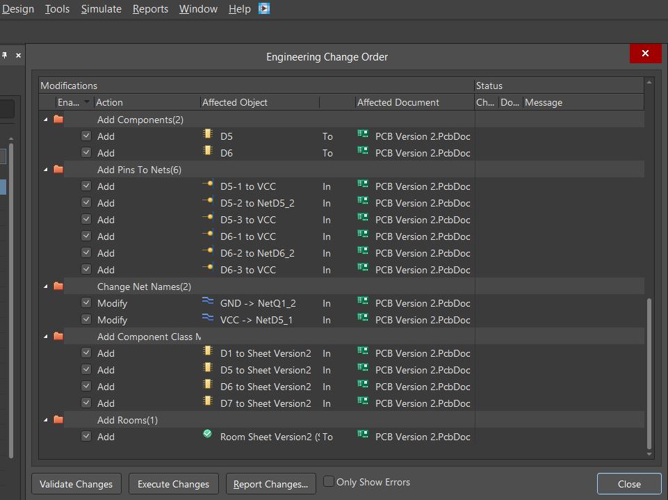
Once the schematic is complete, it’s crucial to ensure it is error-free. After confirming that there are no errors, the next step is to update the PCB. Altium Designer automatically transfers every component and its corresponding connections from the schematic to the PCB layout.
At this point, you’ll notice that all components are connected by thin lines, representing electrical nets. These nets will be routed in the next stages of the design process.
To convert your schematic into a PCB layout, follow these steps:
- Click on Design > Update PCB Document.
- A dialog box will appear, listing all components and their associated nets.
- Click on Validate Change. If all checks pass (green checkmarks), click on Execute Change.
- All components will now automatically appear in the PCB layout.
For simple circuits, a two-layer PCB may suffice. However, multilayer boards are often used for more complex circuits. One of the key benefits of a multilayer board is the inclusion of power and ground planes, which significantly enhance signal integrity.
The most common 4-layer PCB stack consists of the following configuration:
- Top Layer: For components and signals.
- Inner Layer 1: Power plane.
- Inner Layer 2: Ground plane (GND).
- Bottom Layer: For components and signals.
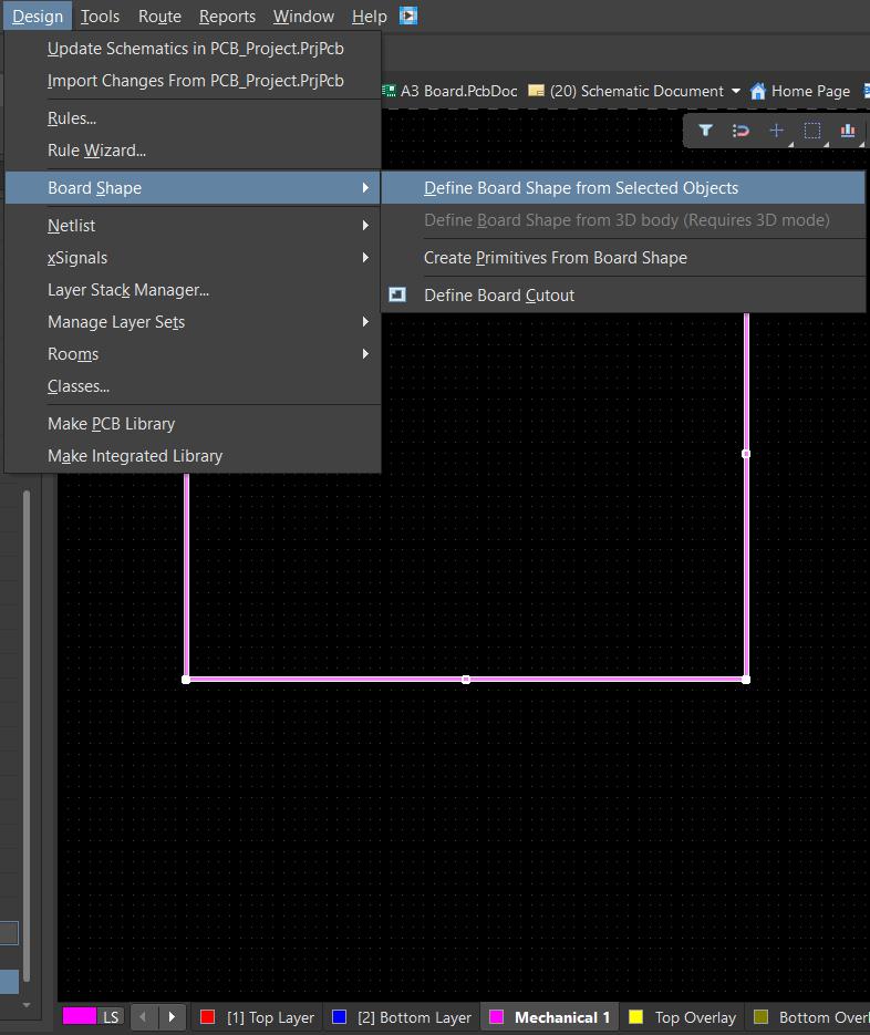
The board size is determined by the mechanical requirements of the assembly or enclosure where the PCB will be mounted.
To define the board shape, follow these steps:
- In the PCB editor, different layers will be shown at the bottom.
- Click on the Mechanical layer.
- Use Place > Line to define the physical outline of the board.
- Then, go to Design > Board Shape > Define from selected objects.
- The board shape will now be defined according to the outline you’ve created.
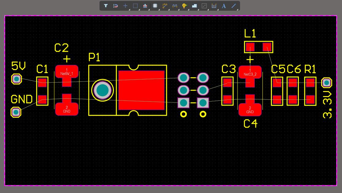
Proper placement not only makes routing easier but also enhances performance and increases the likelihood of a successful PCB. To ensure the best results, follow these professional guidelines:
- Group related components together, such as placing the microcontroller, its crystal, and decoupling capacitors close to each other.
- Place connectors, USB ports, and power jacks near the edges of the board for better accessibility and ease of connection.
- Arrange components in a way that minimizes the use of vias and simplifies the signal flow.
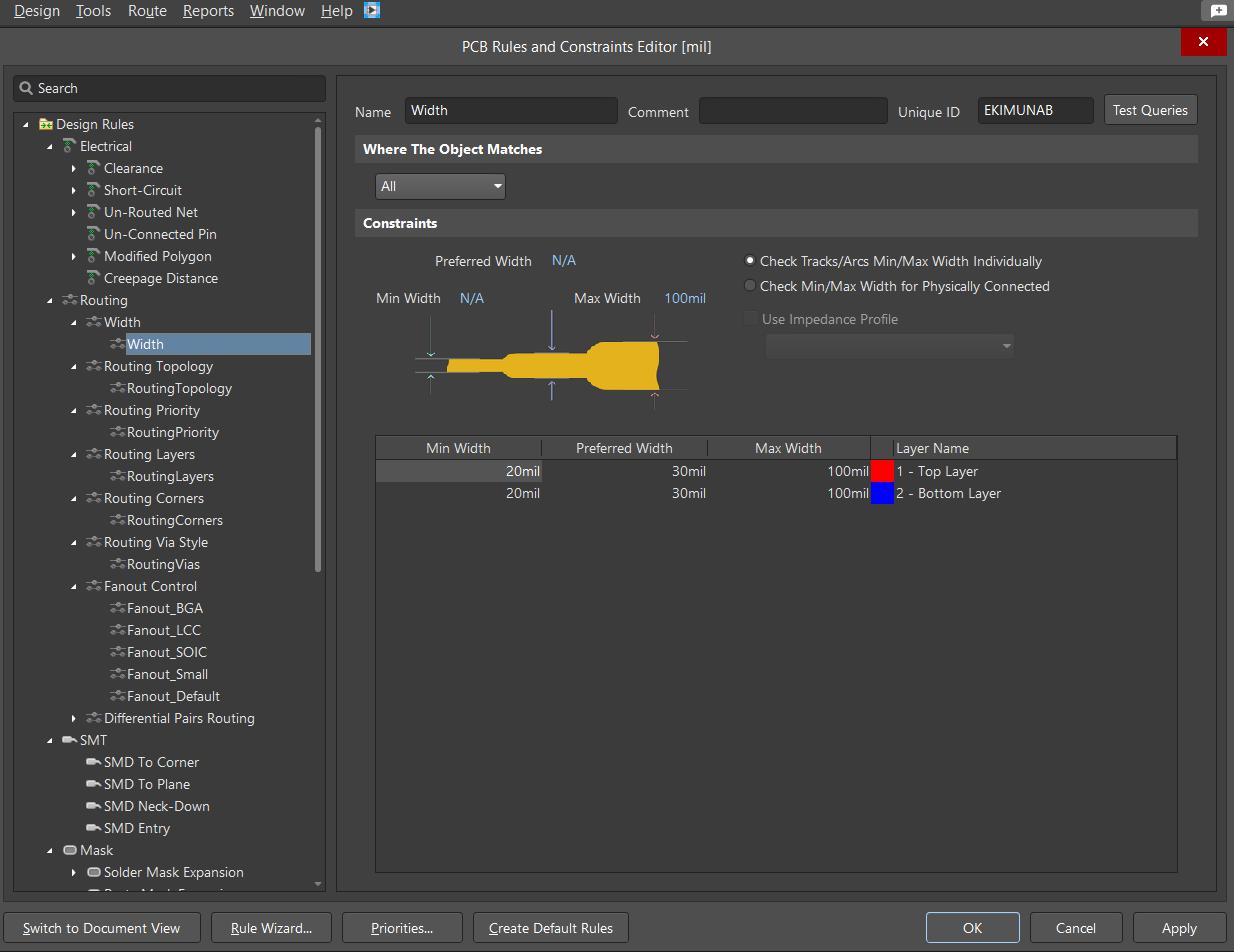
Design rules define minimum track width, pad sizes, and via dimensions. Defining these rules before starting routing not only saves time but also reduces the chance of errors, ensuring that the design can be manufactured reliably.
- Power traces should be wider, while signal traces can be narrower.
- Choose via sizes that are compatible with the manufacturer’s capabilities.
To set design rules, follow these steps:
- Click on Design > Rules.
- A dialog box will appear, displaying various rules that you can adjust to your needs.
- Component Clearance: The standard clearance is 20 mil, but it may vary depending on your board size.
- Routing Width: For power and ground nets, set a width of 30 to 40 mil, and for signal traces, use 20 mil as a default.
- Via Style: Set your via hole size (the preferred size is 0.3mm, with a diameter of 0.6mm).
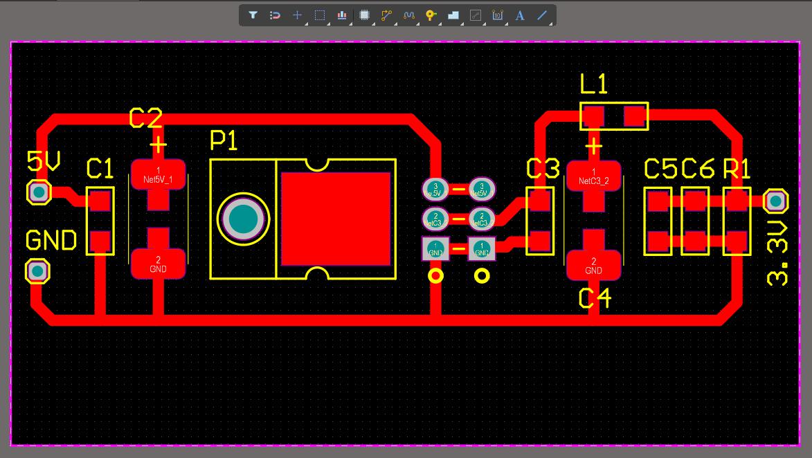
Routing is the process of connecting components using copper traces according to the schematic nets. It’s essential to prioritize power lines first, followed by critical signals, and then the remaining connections.
- Use short, direct paths to minimize signal loss and resistance.
- Avoid sharp angles in traces to prevent signal integrity issues.
- Keep the traces clean and tidy for both aesthetic appeal and electrical efficiency.
- Use vias to switch layers when necessary.
Once routing is completed, add a polygon pour to create a large ground copper area. This helps to reduce noise and improves the board’s overall stability.
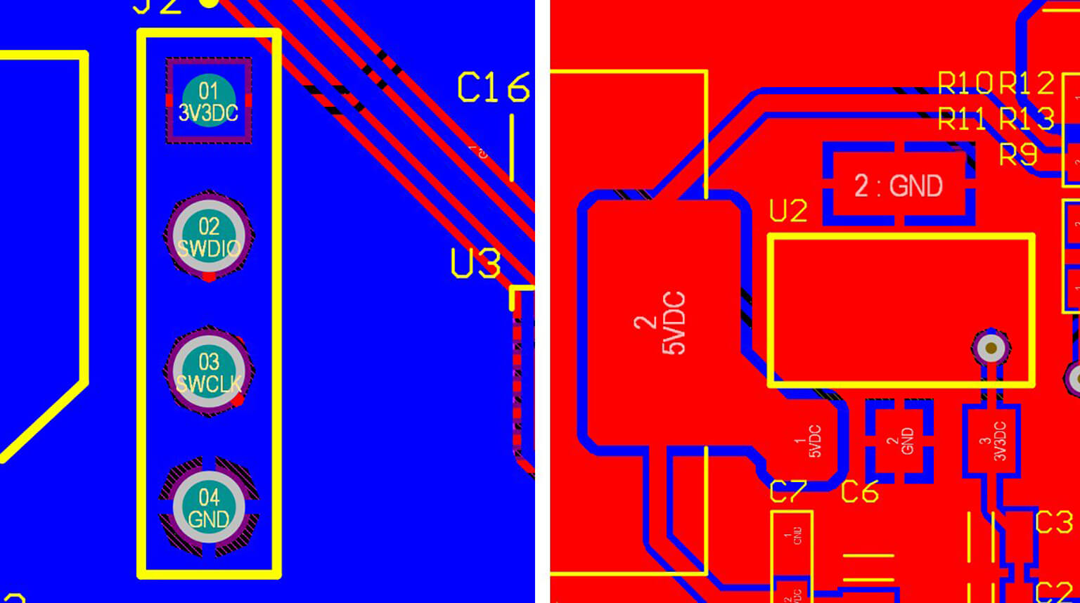
Before generating the final output, it’s essential to run a Design Rule Check (DRC) to identify any errors, such as clearance or routing issues. Carefully review the board to ensure there are no problems that could affect its performance or manufacturability.
Take the time to physically inspect the board in 3D to ensure there’s no overlap of components or other design flaws.
To run the DRC, follow these steps:
- Click on Tools > Design Rule Check.
- Select Run Design Rule Check. The message panel will appear, displaying all errors such as unrouted nets, component clearance, etc.
- Address and correct all identified errors. Once resolved, your PCB will be ready for manufacturing.
This tutorial has walked you through the essential steps of designing a PCB using Altium Designer, from creating a new project to verifying the design before manufacturing. By mastering these steps, you can confidently create high-quality, functional PCB tailored to your specific needs.
Bei PCBCool, we offer comprehensive PCB services, including design, manufacturing, assembly, and more. Whether you’re looking to bring your Altium designs to life or need assistance with the entire process, our expert team is here to help.