
Blog

Alles, was Sie über PCB-Backdrilling wissen müssen

0
PCB-Rückbohrung

If you have ever routed a high-speed differential pair through a 12-, 16-, or 20-layer backplane, you have probably run into a problem that has little to do with trace width or impedance stack-up. That is, the via itself.

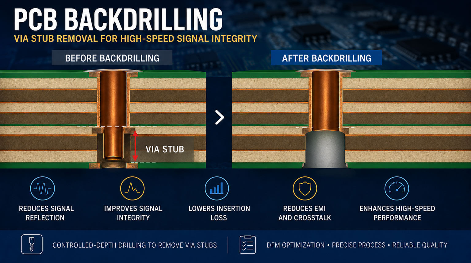
In a conventional multilayer PCB, every plated through-hole (PTH) via is drilled completely through the panel, even if that signal only needs to go from one layer to another near the top. The via stub which is the excess copper that is left behind, turns into a tiny unintended antenna that reflects energy back into your signal path.

For this reason, backdrilling—also known as controlled-depth drilling (CDD)—is used in PCB fabrication to remove that stub. It’s a standard tool in any high-speed designer’s kit and is used everywhere from network switches and server backplanes to radar systems and 224 Gb/s SerDes links.

Whether you are hearing about this process for the first time or evaluating it for a current PCB project, this article will be a useful starting point. Based on our past manufacturing experience, we will begin with the basic concepts and then move into the design-for-manufacturing details needed to specify backdrilling correctly. Let’s begin.

Key Terms in Backdrilling

Before diving into backdrilling itself, let us describe the terminology that is commonly used:

  • PTH — a hole drilled through the entire board and plated with copper to electrically connect two or more layers.
  • Via Stub — the portion of the plated barrel that extends beyond the last layer used by the signal. It carries no signal current but is still electrically connected to the net
  • NPTH — a hole with no copper plating, typically used for mechanical mounting rather than signal routing. Backdrilling doesn’t apply here, since there’s no stub to remove.
  • Don’t-Cut Layer — the deepest (or shallowest) layer the backdrill is allowed to touch; this is the layer your fabricator stops just short of, preserving the connection you actually need.

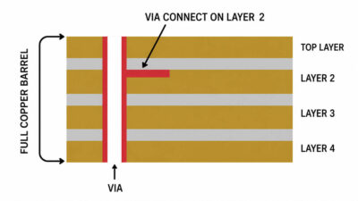
So if you have a 12-layer board and you only need to connect layer 1 to layer 4, a standard PTH via leaves 8 layers of unused copper barrel hanging off the back. That is your stub, and it’s the entire reason backdrilling exists.

Why Backdrilling Is Needed in High-Speed Design

A via stub is basically a short, open-ended transmission line that branches off your actual signal path. This is harmless at low frequencies. Since the stub length is very small compared to the wavelength of the signals, the stub is electrically “invisible”.

However, as data rates increase, the electrical length of the stub becomes a significant fraction of the signal’s rise time, and the stub begins to act like a quarter-wave resonant stub. It reflects energy back toward the source at certain frequencies, creating constructive and destructive interference with the original signal.

The practical symptoms usually show up as:

  • Insertion and Return Loss degradation: At the stubs’ resonant frequency and its odd harmonics, which can carve deep notches directly into your channel’s frequency response.
  • Deterministic Jitter: Since the reflected energy is returned to the receiver with a slight delay relative to the main signal, smearing out the eye pattern
  • Increased Bit Error Rate (BER): It is the direct consequence of a closed or distorted eye at the receiver.
  • Via-to-via Crosstalk: Because the stub acts as a small radiating element that couples energy into neighboring nets.
  • EMI/EMC Issues: For the same reason, an unterminated stub doesn’t just pick up noise; it can radiate it.

As a rule of thumb, designers start paying close attention to stub effects once data rates climb past roughly 2.5 – 3 Gbps per lane, and backdrilling becomes almost a requirement above 5-10 Gbps, or for any RF/microwave design operating in the multi-GHz range. The exact threshold really depends on your stack up, dielectric, and rise time, which is why signal integrity simulation (not just a rule of thumb) is the actual right way to make the final decision on any given net.

PCB Backdrilling Process Steps

Backdrilling happens after the board has already been drilled and plated. It is a secondary process of controlled depth and is not a replacement for normal fabrication.

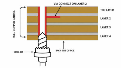
  1. Standard Drilling and Plating

The board undergoes its standard PTH drilling and copper plating cycle, resulting in a completely connected barrel from one end of the board to the other, just like for any standard via.

Standard Drilling and Plating
  1. Backdrill Setup and Registration

The fabricator aligns the panel using optical or mechanical registration so the backdrill bit can be positioned precisely over the center of the existing via

Backdrill Setup and Registration
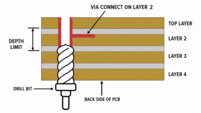
  1. Controlled-Depth Re-Drilling

A drill bit, slightly larger in diameter than the original via, typically 8-10 mil oversize, reenters from the side opposite the signal source and bores down to a tightly controlled Z-axis depth, removing the plated copper in the stub region.

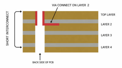
  1. Stopping Before the Do-Not-Cut Layer

The drill stops just before reaching the last connected layer, leaving a small residual stub (commonly under 10 mil, with high-performance designs pushing toward 2–5 mil) to protect the integrity of the remaining pad and barrel.

Stopping Before the Do Not Cut Layer
  1. Hole Cleaning and Optional Filling

Clear the hole of drilling debris. Many fabricators epoxy-fill backdrilled holes. This is not strictly necessary but it produces a more consistent result and prevents debris from interfering with assembly later on.

  1. Inspection and Verification

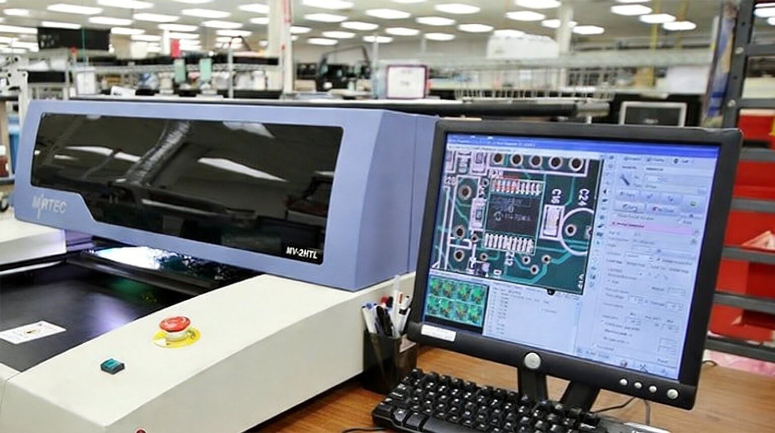
Cross-sectioned coupons or X-ray inspection confirm that the backdrilled depth and residual stub length meet the specified tolerance.

The result is a via that electrically behaves almost like a true blind via for the signal layers you care about, without the added cost of laser drilling or sequential lamination.

Schematic diagram showing the final result of a backdrilled PCB

Design Parameters You Need to Specify

This is where many designs go wrong. Backdrilling is only as good as the data package you give your fabricator. At a minimum, your fabrication drawing or stack-up file should define the following:

ParameterTypical Guideline
Backdrill oversizeOriginal via diameter + 8–10 mil (smallest practical backdrill diameter is roughly 18 mil; anything smaller breaks easily)
Residual stub length≤ 10 mil for standard designs; 2–5 mil for advanced, high-speed designs (a true zero-length stub isn’t achievable as it would compromise the pad/barrel connection)
Depth toleranceTypically ±2 mil on the controlled drill depth
Backdrill-to-copper clearance~10 mil minimum from the oversized hole to adjacent traces or planes on a different net
Backdrill-to-backdrill clearance~6 mil minimum between adjacent backdrilled holes
Dielectric margin to the do-not-cut layerAt least 10 mil of dielectric between the drilled-from surface and the don’t-cut layer, to leave enough margin for both the minimum drill depth and tolerance

A few practical notes that matter just as much as the numbers:

  • Specify the don’t-cut Layer, not a depth in mils. Telling your fabricator to “stop after layer 4” is a better instruction than specifying a Z-axis distance, because the fabricator controls the actual stack-up tolerances and press cycle variation.
  • State which side the backdrill enters from for every span, top or bottom, since this is not always clear from the layer pair alone.
  • Only backdrill the nets that require it. High-speed differential pairs and other signal-critical nets are candidates. Power and ground vias should generally just be left alone, since the cost of backdrilling scales with the number of distinct depths and hole counts on the panel.
  • Add keep-outs on the exit side. The oversized backdrilled hole means no traces, planes, or components can sit directly beneath it on the side the drill enters from.

Specifying Backdrilling in Your CAD Tool

Most modern PCB design tools, e.g., Altium Designer, Cadence OrCAD/Allegro, and KiCad, support backdrilling through dedicated padstack or layer-stack features rather than treating it as a manual annotation.

Regardless of the tool used, the general workflow looks like:

  1. Define the backdrill as a feature in your layer stack-up or padstack editor, specifying the start layer (entry side) and the don’t-cut layer.
  2. Create a net class or net group containing only the high-speed nets that require backdrilling. This keeps the rule from accidentally applying to power/ground vias.
  3. Set design rules for maximum stub length, backdrill oversize, and clearance to other copper, scoped to that net class.
  4. Route normally, then run a design rule check (DRC) to confirm every via on a backdrilled net actually picked up the correct feature.
  5. Generate a drill table or backdrill chart as part of your fabrication output. Do NOT leave the fabricator to infer your intent from the layer stack alone. A clear drill chart with hole counts per depth avoids costly miscommunication.

It’s worth visually verifying the result before sending files out. Most tools will display backdrilled vias with a dual-color ring (one color for the entry layer, another for the don’t-cut layer), making it easy to spot vias that didn’t get the rule applied correctly.

Backdrilling vs. Alternatives

AnsatzHow it Solves the Stub ProblemTrade-offs
BackdrillingMechanically removes the unused barrel after plating.Adds a drilling step and cost;
Residual stub still exists (though minimal);
Works on standard PTH boards.
Blind/buried viasVia never extends past the layers it needs to connect.No residual stub at all;
Requires sequential lamination;
Raising the cost and lead time significantly.
Microvias (HDI)Laser-drilled, layer-pair-specific connections.Excellent for fine-pitch, high-density routing;
Not always practical for thick backplanes or high layer counts.
Stack-up rearrangementRoute critical high-speed layers closer to the via’s natural stub-free end.Free if planned early;
Constrains the rest of your stack-up and routing strategy.

Backdrilling is not the only way to deal with via stubs, but it remains a primary choice for standard multilayer PCB—especially for thick backplanes and midplanes, where blind and buried vias are often impractical or too costly to justify.

Advantages and Limitations

Vorteile:

  • Greatly improved signal integrity of high-speed digital and RF designs.
  • Much cheaper than redesigning a stack-up for blind/buried vias or HDI microvias.
  • Compatible with standard multilayer PCB fabrication without exotic processes
  • It is selectively applied hence it scales well across many nets on a single board.

Einschränkungen

  • Adds a manufacturing step and thus costs, which scale with the number of different backdrill depths.
  • The oversized hole on the exit side uses upboard space. No routing or component placement is allowed there.
  • Some fabricators are not able to consistently achieve the tight Z-axis control that is necessary to get ultra-short residual stubs (< 5 mils).
  • There’s always a residual stub, however small, that is not an ideal stand-in for a real blind via.

Our PCB Backdrilling Capabilities

ArtikelBefähigung
Schichtanzahl4–40 layers
Board Thickness & Size0.8–6.5 mm; up to 620 × 720 mm
MaterialienFR-4, High-Tg FR-4, Rogers, Taconic, Isola, Panasonic, Nelco, mixed lamination
Min. Mechanical Drill Before Backdrilling0,15 mm
Backdrill DiameterOriginal PTH drill size + 0.20–0.25 mm
Min. Backdrill Diameter0.30–0.35 mm
Backdrill Depth Tolerance±0.05 mm standard; ±0.03 mm by engineering review
Residual Stub Target≤0.25 mm standard; 0.05–0.13 mm advanced
Backdrill Clearance≥0.25 mm to copper standard; ≥0.15 mm backdrill-to-backdrill standard
Backdrilling SupportTop-side, bottom-side, both-side, multiple backdrill depths, DFM review, cross-section, coupon inspection, X-ray, impedance test

Abschließende Gedanken

Backdrilling is not a “fire and forget”. A good fabricator should validate the result with appropriate inspection methods, such as cross-sectioned coupons or X-ray inspection, to confirm that the residual stub length meets the specified requirement and that the inner-layer copper near the do-not-cut layer has not been nicked, exposed, or damaged.

For high-speed or reliability-sensitive PCB projects, verification requirements should be discussed before fabrication starts. IPC-6012 provides qualification and performance requirements for rigid PCBs, but the exact coupon plan, inspection method, and reporting requirements should also be confirmed with your fabricator based on the board stack-up and the number of unique backdrill depths.

If you are working with a new fabricator or a high-speed multilayer design, it is worth requesting backdrilling verification data as part of the standard manufacturing deliverables. At PCBCool, our engineering team reviews the stack-up, do-not-cut layer, residual stub target, drill side, and inspection requirements during the DFM stage, helping customers reduce signal integrity risk before the board reaches production.

Häufig gestellte Fragen

Q1: Warum hat die Lagenanzahl einen so großen Einfluss auf die Kosten von Leiterplatten?

Der Hauptgrund dafür ist, dass jede zusätzliche Schicht den Herstellungsprozess schwieriger zu kontrollieren macht. Mehr Schichten bedeuten mehr Möglichkeiten für Defekte in den inneren Lagen, Ausrichtungsprobleme, Laminationsprobleme und Ausschuss.

Warum erfordern BGA-Designs eine strengere Kontrolle der Leiterplattenherstellung?

A: BGA-Pads sind klein und eng beieinander angeordnet, sodass kleine Herstellungsfehler leicht zu Montageproblemen werden können.

Sam K
Sam K | Embedded Systems Engineer

Sam K arbeitet an eingebetteten elektronischen Systemen mit Schwerpunkt auf Hardware-Design, PCB-Entwicklung, Firmware-Programmierung und Systemintegration. Er unterstützt auch die Leistungsoptimierung und hilft bei der Umsetzung von Ideen für elektronische Produkte in zuverlässige, praxistaugliche Lösungen.

Verwandte Schlagwörter