Single-board computers have become increasingly popular in industrial automation, edge computing, and embedded AI applications. While off-the-shelf platforms provide a convenient starting point, many commercial products require custom hardware tailored to specific mechanical, electrical, and connectivity requirements. In such cases, System-on-Module (SOM) solutions offer a practical balance between development effort and system flexibility.
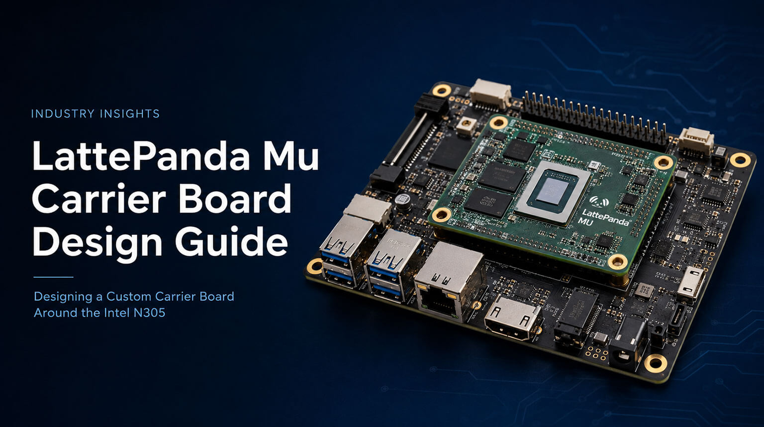
The LattePanda Mu is a compact x86-based SOM powered by Intel’s Alder Lake-N processor family, including the Intel N305. Unlike traditional single-board computers, this module integrates the CPU, memory, storage, and power management circuitry into a compact form factor, allowing designers to focus primarily on application-specific carrier board development.
Recently, PCBCool designed a custom carrier board for the LattePanda Mu platform. The objective was to create a robust and expandable hardware platform capable of exposing high-speed interfaces while maintaining reliable signal integrity and power delivery. Although the SOM significantly simplifies system development compared to designing a full x86 motherboard, the carrier board still presents several engineering challenges.
Before schematic design began, several project requirements were defined to guide the hardware architecture.
The LattePanda Mu carrier board needed to expose multiple external interfaces while maintaining a compact PCB footprint.
The primary design goals included:
- Reliable power delivery for the LattePanda Mu
- PCI Express Gen3 expansion capability
- Gigabit Ethernet networking
- USB 3.0 connectivity for high-bandwidth peripherals
- USB 2.0 connectivity for medium-bandwidth peripherals
- USB-C DisplayPort Alt Mode output for external displays
- HDMI output for external displays
- General-purpose I/O access for embedded control applications
- Compact mechanical form factor
Because the CPU, memory subsystem, and storage resources are already integrated within the module, the design effort could focus on interface implementation and PCB layout optimization rather than complex processor support circuitry.
The overall system architecture is centered on the LattePanda Mu as the primary processing engine, while the carrier board defines how the system connects to external devices, displays, networks, expansion modules, and power sources.
This makes the carrier board a critical part of the final hardware platform rather than a simple breakout board.
Input power is supplied through an external DC source and distributed through multiple power rails required by peripheral devices and expansion interfaces. While the SOM handles its own internal power sequencing, sufficient current capacity and low-noise power distribution remain important for stable operation under varying computational loads.
For this reason, the carrier board power architecture was designed to support both the LattePanda Mu module and the external interfaces connected to the board. USB ports, Ethernet circuitry, display interfaces, and expansion connectors all place additional requirements on the power distribution network.
Several high-speed interfaces are routed directly from the SOM to external connectors. USB 3.0 channels provide support for high-bandwidth peripherals, while DisplayPort and HDMI outputs enable connection to external monitors and industrial display systems. Gigabit Ethernet provides network communication, and PCIe lanes are routed to an expansion connector for future hardware integration.
From a PCB layout perspective, these interfaces represent the most critical portion of the design because signal integrity requirements become increasingly important as data rates rise into the multi-gigabit range.
As a result, PCB stackup selection, impedance control, differential pair routing, and return-path management were considered from the earliest stages of the design process.
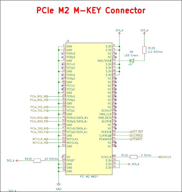
PCI Express Gen3 links operate at 8 GT/s, making them highly sensitive to impedance discontinuities, excessive skew, and poor return current paths.
All PCIe differential pairs were routed using controlled impedance traces based on PCI-SIG recommendations. The target differential pair impedance was 85 Ω ±15%. Differential pair spacing and trace width were adjusted to achieve the required impedance while maintaining consistent coupling throughout the routing path.
Special attention was given to minimizing discontinuities introduced by vias and layer transitions. Differential pairs were always routed on the same layer, and split return paths were avoided. When a differential pair needed to change layers, nearby ground stitching vias were added to provide a continuous return path and reduce electromagnetic radiation.
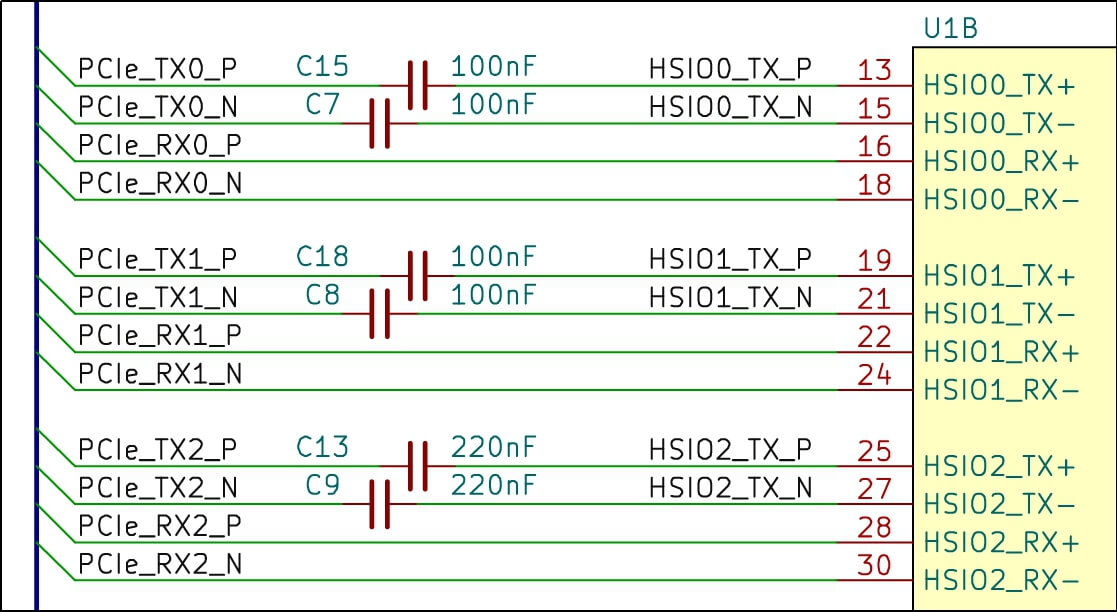
AC-coupling capacitors were placed on the PCIe transmitter lanes according to PCI-SIG recommendations. These capacitors block DC voltage differences between communicating devices while allowing the high-frequency differential data stream to pass without distortion.
Proper capacitor placement is critical because excessive distance from the transmitter can introduce unwanted signal degradation. In this design, small package capacitors, such as 0402 or smaller, were preferred to minimize pad impedance mismatch and keep the AC-coupling path compact.
To further improve signal quality, routing stubs were avoided and connector placement was optimized to minimize total channel length. If test access is required, stubs should be avoided and test points should be placed on the signal trace.
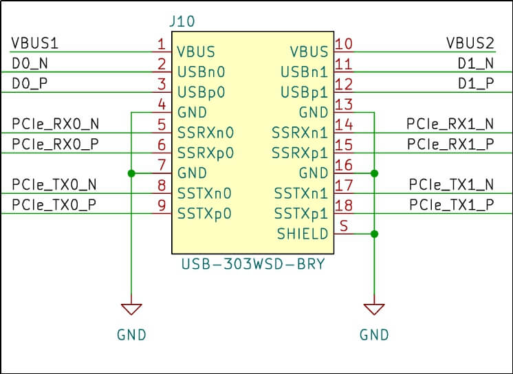
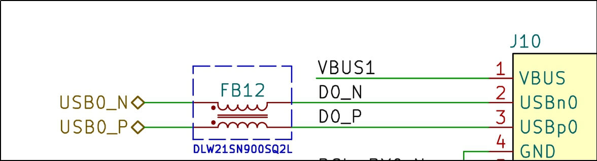
The carrier board provides two USB 3.0 Type-A ports for high-bandwidth peripherals such as external SSDs, industrial cameras, and data acquisition devices. Each USB 3.0 Type-A port includes both USB 2.0 D+/D− data lines and USB 3.0 SuperSpeed differential pairs.
USB 3.0 SuperSpeed signals operate at 5 Gbps and require many of the same layout techniques used for PCIe routing, although the target differential impedance is different. Differential impedance control, pair length matching, and continuous reference planes were maintained throughout the routing process.
AC-coupling capacitors were placed on the SuperSpeed transmit pairs according to USB interface requirements. Similar to PCIe, these capacitors isolate common-mode voltage differences between connected devices while preserving the integrity of the differential signal.
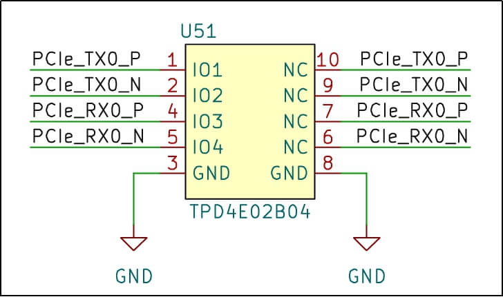
Because USB connectors are frequently exposed to direct user interaction, electrostatic discharge protection was a significant design consideration. For high-speed interfaces, low-capacitance ESD protection devices were placed immediately adjacent to the connector interface to reduce the risk of damage during cable insertion and handling while minimizing signal degradation caused by parasitic capacitance.
In this design, different Texas Instruments ESD protection devices were used for USB 3.0 and USB 2.0 data lines. One is TPD4E02B04 for USB 3.0 data lines because it satisfies 0.25 pF low junction capacitance and 3.6 V reverse stand-off voltage. The other is ESDS452 for USB 2.0 data lines, which has 3 pF junction capacitance and 5.5 V reverse stand-off voltage.
EMI performance was improved by maintaining uninterrupted ground reference planes beneath all SuperSpeed differential pairs and minimizing unnecessary layer transitions. Common-mode chokes can be placed on USB 2.0 D+/D− lines to reduce common-mode noise, but they should generally be avoided on USB 3.0 SuperSpeed lines unless their high-speed performance has been carefully validated.
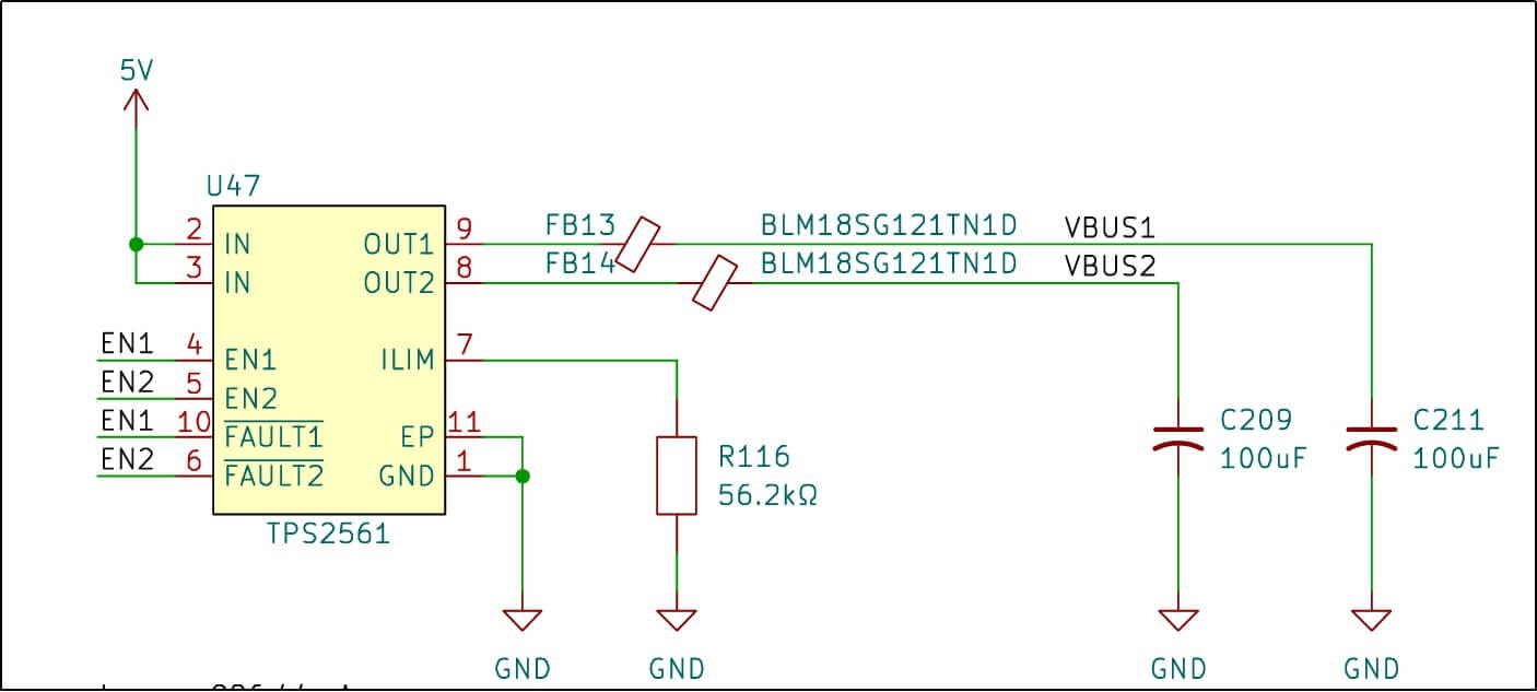
VBUS protection was also required because external USB devices may draw excessive current or behave as a short circuit. If this occurs, the USB power path can stress the carrier board’s power distribution network, potentially damaging power circuitry or triggering unwanted system resets.
To prevent this, the Texas Instruments TPS2561 USB power switch was used for VBUS current limiting and fault protection. In this design, each USB port’s maximum allowable current was set to 1 A.
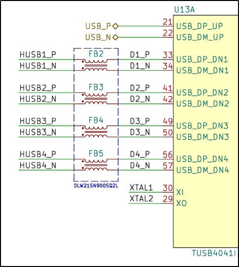
The LattePanda Mu provides a limited number of native USB 2.0 interfaces. To increase peripheral connectivity, a TUSB4041I-Q1 USB hub controller was incorporated into the carrier board design.
Although USB 2.0 operates at lower signaling speeds than PCIe or USB 3.0, signal integrity considerations remain important. Differential routing practices were maintained, and ESD protection devices were implemented at all externally accessible ports.
The hub controller near the center of the USB topology helped reduce trace lengths and simplify routing while maintaining reliable communication across all downstream ports.
One of the more complex portions of the design was implementing DisplayPort Alt Mode through a USB Type-C connector.
The design used a TUSB422 Type-C port controller together with a TUSB546A high-speed multiplexer. The TUSB422 manages CC channel communication, cable orientation detection, and Alt Mode negotiation. Once the cable orientation is determined, the TUSB546A routes the DisplayPort lanes to the appropriate USB Type-C pins.
DisplayPort signals operate at multi-gigabit data rates and therefore require strict impedance control and careful routing practices. Differential pair length matching, reference plane continuity, and via optimization were treated as high-priority design requirements.
AC-coupling capacitors were implemented on the DisplayPort transmitter lanes to eliminate DC bias differences between connected devices. In addition, ESD protection was applied to the high-speed lanes, AUX, HPD, and CC-related lines to improve system robustness against external discharge events.
Because the USB Type-C connector is typically located near the edge of the PCB, maintaining good EMI performance required careful attention to return current paths, connector grounding, and shield connection strategy.
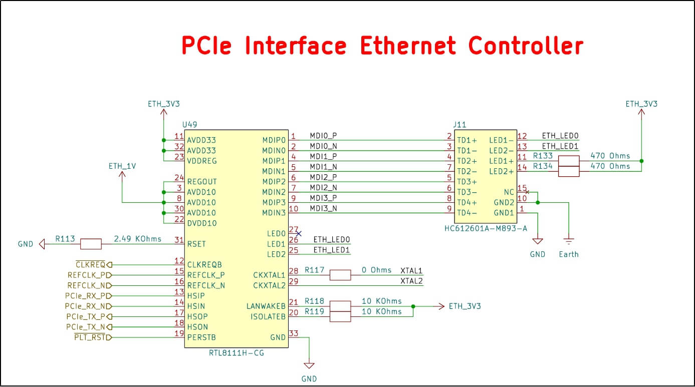
Network connectivity was implemented using the RTL8111H-CG Gigabit Ethernet controller. In this design, the controller connects to the LattePanda Mu through a PCIe interface and converts the PCIe link into Gigabit Ethernet MDI differential pairs.
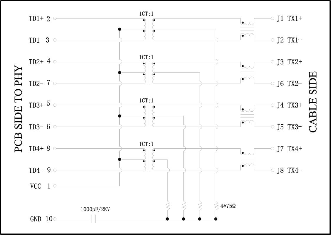
The Ethernet differential pairs between the controller and the magnetic module were routed with controlled impedance and matched electrical lengths. Placement of the Ethernet controller, magnetics, and RJ45 connector was optimized to reduce routing complexity and minimize noise coupling from nearby high-speed interfaces.
ESD protection devices were positioned near the RJ45 connector to protect against cable discharge events. The Ethernet magnetics provide galvanic isolation between the PCB side and cable side while also contributing to improved electromagnetic compatibility.
A SOM such as the LattePanda Mu can greatly reduce the complexity of x86 hardware development, but the carrier board is what turns the module into a usable product platform. Its role is not only to expose interfaces, but also to bring together power delivery, signal integrity, protection, layout control, and manufacturability into one reliable hardware system.
For teams developing custom carrier boards or SOM-based products, PCBCool can support the process from engineering review and controlled-impedance PCB fabrication to PCB assembly, inspection, and testing, helping hardware projects move more smoothly from design to production.