The Internet of Things has fundamentally changed how electronic systems are designed. Unlike traditional embedded boards, IoT devices must carefully balance low power consumption, wireless connectivity, compact form factor, reliability, and regulatory compliance — all while keeping costs under control.
Simply creating a functional circuit is no longer sufficient. A well-designed IoT PCB must:
- Deliver consistent RF performance
- Operate for months or even years on a single battery
- Meet EMC and other certification standards
- Endure harsh real-world conditions
- Be practical to manufacture at scale
This guide is intended for engineers who want to go beyond basic PCB design and gain a deeper understanding of the practical challenges involved in developing robust IoT hardware.
Choosing the right power source is one of the first and most critical decisions in an IoT PCB project:
Most common for true IoT devices, options include single-cell LiPo/Li-ion (3.7–4.2 V), coin cells (e.g., CR2032 for ultra-low-power designs), or AA/AAA with boost converters. This choice affects voltage rails, charging circuitry, and sleep current targets.
Ideal for development, always-on, or hybrid devices. Provides 5 V input, simplifies debugging, and often supports device charging. Requires careful power path management to switch seamlessly between sources.
- Solar / Energy Harvesting:
Ideal for remote sensors such as environmental monitors. Requires MPPT (Maximum Power Point Tracking) ICs, supercapacitors or small batteries for energy storage, and ultra-low-power design techniques.
The combination of battery, solar, and USB fallback — common in industrial IoT (IIoT) deployments – balances autonomy, reliability, and cost.
The choice of wireless protocol is often the biggest differentiator in IoT devices:
- BLE (Bluetooth Low Energy):
Short-range (~10–100 m), extremely low power, suited for wearables, beacons, and phone pairing (e.g., nRF52840, ESP32).
Offers higher bandwidth and direct internet access but consumes more power, making it suitable for smart home devices and cameras (e.g., ESP32, ESP8266).
Long-range (kilometers), ultra-low-power, low data rate—ideal for remote sensors, agriculture, or asset tracking (e.g., STM32WLE5, SX126x modules).
Cellular connectivity for wide-area coverage without gateways, but with higher cost, power, and certification complexity (e.g., Quectel BG95, SIM7000).
Zigbee, Thread, Sigfox, etc., depending on ecosystem requirements.
Identify every sensor and its communication interface early. This determines GPIO requirements, bus loading, pull-ups, noise filtering, and power sequencing:
Multi-device bus (e.g., temperature/humidity sensors like SHT4x, IMUs like MPU6050). Requires pull-up resistors (typically 4.7 kΩ) and supports multiple slave devices.
High-speed, point-to-point or daisy-chain interface (e.g., SD cards, displays, high-speed ADCs). Uses more pins (MOSI, MISO, SCK, CS).
Direct analog inputs for simple sensors (e.g., potentiometers, light sensors, battery monitoring). Consider resolution, reference voltage, and noise.
Used for GPS modules, debug consoles, or legacy sensors.
One-wire (DS18B20), PWM, GPIO interrupts for wake-up events.
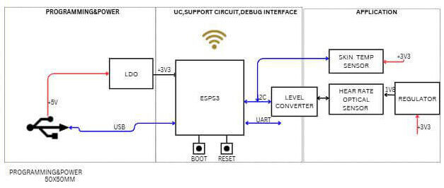
Before diving into circuit schematics, draw a clear block diagram using tools like draw.io, Lucidchart, or even paper. The diagram should illustrate:
- Power flow: Source → regulators → functional domains
- Data flow: Sensors → MCU → connectivity → cloud
- Control signals: Enable pins, interrupts
- Key ICs and interfaces
This visual becomes your single source of truth, essential for alignment across firmware, hardware, and mechanical teams.
Example block diagrams can help illustrate typical IoT architectures and guide your design process.
This is a major fork in the road—requiring a balance between cost, time-to-market, and design complexity.
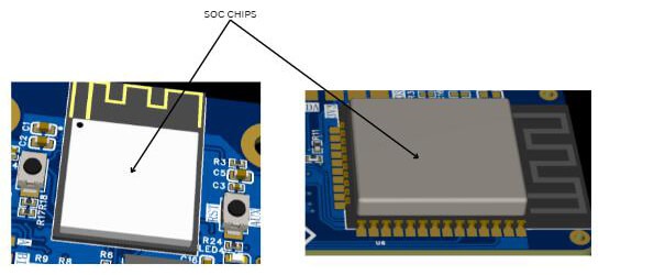
Such as the ESP32-WROOM, nRF52840 module, Quectel cellular modules, or Seeed LoRa-E5, provide a quick path to regulatory approval.
Vorteile
- Already certified for FCC/CE/RED/TELEC, which greatly speeds up compliance.
- Integrated antenna matching, crystal, and RF shielding simplify design.
- Easier PCB layout, with fewer strict RF guidelines to follow.
- Often include built-in flash, voltage regulators, and essential passive components.
Nachteile
- Higher unit cost compared to a bare SoC.
- Larger footprint, which may limit compact designs.
- Reduced flexibility due to fixed pinout and, in some cases, locked firmware.
Best Use Cases:
Ideal for first prototyping, products that need rapid market entry, or teams without deep RF design expertise.
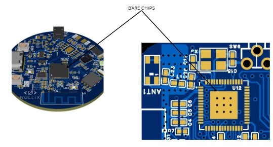
Such as a raw ESP32 die, STM32 paired with a separate radio, or Nordic nRF5340, offer maximum customization at the cost of design complexity.
Vorteile
- Lowest BOM cost when produced in high volumes.
- Full flexibility for pin assignment, firmware, and feature integration.
- Potential for smaller overall size with careful layout and component placement.
Nachteile
- Requires complex RF layout, including controlled 50 Ω traces, ground planes, via stitching, and antenna tuning.
- Certification is the designer’s responsibility, which can be expensive and time-consuming.
- Additional passive components and crystals are usually required.
Best Use Cases:
Suitable for high-volume production, ultra-compact designs, or projects that demand custom optimizations not possible with pre-certified modules.
Battery life is often the primary constraint in IoT devices. Consider both active current (during processing or radio transmission) and sleep current (deep sleep modes).
Decide whether the MCU includes an integrated radio such as WiFi, BLE, or LoRa. Integrated RF simplifies PCB layout and reduces BOM cost, but may limit flexibility. Check the transmit power (e.g., +20 dBm for long-range communication) and receiver sensitivity (e.g., -100 dBm for detecting weak signals).
Firmware complexity dictates flash and RAM needs. Simple sensor applications may require only 256 KB Flash and 64 KB RAM, whereas AI/ML edge processing can demand 4 MB+ Flash and 512 KB+ RAM. Always consider extra memory for OTA updates.
Make sure the MCU has enough pins for sensors (I²C, SPI, ADC), debugging interfaces (SWD, UART), and peripherals. Multiplexing can help, but too few pins may necessitate external multiplexer chips, adding complexity.
A strong software ecosystem—including SDKs, libraries, and development tools—can significantly speed up coding, debugging, and OTA update workflows. Popular MCUs often benefit from active communities, example projects, and IDE plugins.
| Merkmal | ESP32-S3 | nRF5340 | STM32WL |
|---|
| Core | Dual-core Xtensa LX7 @ 240 MHz with AI accelerators | Dual-core Arm Cortex-M33 (app 128 MHz / net 64 MHz) | Arm Cortex-M4 @ 48 MHz + Cortex-M0+ for radio |
| Active / Sleep Current | 100–200 mA (WiFi TX) / ~10 µA | 5–10 mA (BLE TX) / 0.3 µA | 15–30 mA (LoRa TX) / 1 µA |
| RF Integration | WiFi 802.11b/g/n + BLE 5.0; +20 dBm TX | BLE 5.2, Zigbee, Thread; +8 dBm TX | LoRa, (G)FSK; +22 dBm TX (sub-GHz) |
| Flash / RAM | Up to 16 MB Flash / 512 KB SRAM + 8 MB PSRAM | 1 MB Flash / 512 KB RAM (app) + 256 KB RAM (net) | 256 KB Flash / 64 KB RAM |
| GPIO Count | Up to 45 (multiplexed) | Up to 48 (multiplexed) | Up to 43 (multiplexed) |
| Ecosystem | ESP-IDF (C/Python), Arduino support, strong community, VS Code plugin | nRF Connect SDK (Zephyr RTOS), BLE tools, Segger J-Link | STM32Cube, LoRaWAN stack, Keil/STM32CubeIDE, industrial-grade |
| Am besten für | Smart home, AI edge (voice/image), WiFi/BLE devices | Low-power mesh networks, wearables, BLE/Thread | Long-range sub-GHz (metering, agriculture), energy-harvesting |
| Approx. Price | $2–4 (volume) | $4–6 (volume) | $3–5 (volume) |
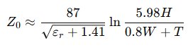
Maintaining controlled impedance is essential for RF signals to propagate without reflections, preserving signal integrity. The characteristic impedance (Z₀) depends on:
- Trace width (W)
- Height above ground plane (H)
- Dielectric constant (εr)
- Copper thickness (T)
For most IoT PCB designs, a 50 Ω target is standard. Mismatched impedance can cause VSWR >1.5, resulting in power loss or unwanted emissions.
Design Tools: Polar SI9000, AppCAD, or online calculators. For a microstrip line, a common formula is:
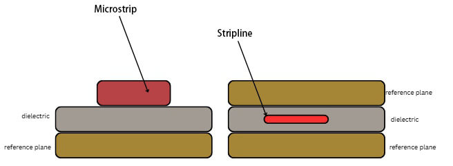
When designing IoT PCB RF traces, treat them as transmission lines. Two common types are microstrip and stripline:
| Aspekt | Mikrostrip | Stripline |
|---|
| Struktur | Trace on top layer above ground plane (exposed to air) | Trace sandwiched between two ground planes |
| Vorteile | Easier fabrication, lower cost, accessible for tuning | Better shielding, consistent impedance |
| Konsens | More susceptible to external interference, higher loss | Harder to access or tune, requires more layers |
| Impedance | Affected by air (effective εr lower) | Fully embedded (uses full εr) |
| IoT Use | Simple 2–4 layer boards (e.g., BLE antenna feed) | High-density RF modules or multi-radio designs |
| Loss | Higher dielectric loss due to air interface | Lower loss, though via transitions can add stubs |
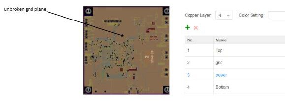
A solid, unbroken ground plane acts as the RF return path and a mirror for signals. Key guidelines:
- Use at least a 4-layer stack with dedicated GND layers under RF sections.
- Avoid splits or slots under RF traces, which create impedance discontinuities.
- Pour GND on all layers and interconnect with vias. For multi-band designs, segmentation is acceptable if stitched heavily.
IoT Tip: In battery-powered devices, integrate power planes but isolate them from RF ground to avoid noise coupling.
Vias connect ground planes across layers, creating low-impedance paths and additional shielding:
- Platzierung Every λ/20 along RF traces or board edges (e.g., ~6 mm at 2.4 GHz).
- Types: Through-hole for simple designs; blind or buried for HDI boards.
- Typical diameter: 0.2–0.3 mm with 0.15 mm annular ring.
Purpose: Prevent resonances, reduce EMI leakage, and, in coplanar lines, stitch both sides for CPWG.
Avoid: Vias in signal paths (creates stubs); back-drill if necessary.
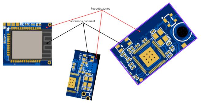
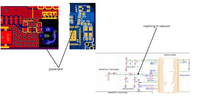
Antenna is responsible for radiating/receiving EM waves; its placement directly impacts the efficiency of IoT PCB (target efficiency η > 50%):
- Place antennas at board edges or corners, away from metal objects like batteries, shields, or connectors.
- Maintain a minimum clearance of 5–10 mm from nearby components. For MIMO setups, keep antennas >λ/2 apart.
- No ground directly under the radiating element.
- Orient antennas according to polarization (vertical for monopoles).
- Use EM simulation tools to predict radiation patterns and VSWR.
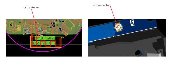
Etched on the board (e.g., Inverted-F or meander). Compact and low-cost, typically offering 2–3 dBi gain. Sensitive to surroundings, so tuning with a matching network is recommended. Ideal for small IoT devices such as sensors.
Higher gain (5+ dBi), flexible form factor (whip, chip), but higher cost and requires a connector. Use for applications where range is critical.
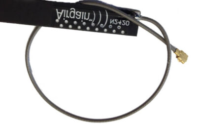
U.FL Connectors
Miniature coaxial connectors used for external antennas or test points. Solder to 50 Ω trace ends, often paired with pigtail cables. Supports frequencies up to 6 GHz. Proper grounding is essential to maintain shielding. Common in modules like ESP32 with antenna switching.
For maximum power transfer between the RF source and antenna, design a π or L matching network. Proper tuning compensates for PCB layout parasitics and ensures VSWR is within acceptable limits.
When selecting a battery, consider factors such as energy density, safety, cost, temperature tolerance, and cycle life.
| Chemistry | Nominal Voltage | Energy Density | Sicherheit | Cycle Life | Typical IoT Use Case | Key Drawback |
|---|
| Li-ion (18650 / 21700) | 3.6–3.7 V | Very high (~250 Wh/kg) | Moderate (requires protection) | 500–1000 cycles | High-power devices such as cameras or gateways | Potential thermal runaway if abused |
| LiPo (pouch cell) | 3.7 V | Very high, flexible form factor | Low–Moderate | 300–500 cycles | Wearables and compact sensors | Can swell if over-discharged or stressed |
| LiFePO₄ (prismatic) | 3.2 V | Lower (~160 Wh/kg) | Excellent | 2000–5000 cycles | Industrial or solar-powered IoT sensors | Larger and heavier for the same capacity |
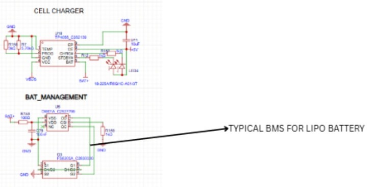
For single-cell lithium batteries, a Protection Circuit Module (PCM) or battery management chip is essential. A common low-cost solution is the DW01 + 8205A protection pair.
LDO regulators are typically used for always-on rails, low-current loads (usually below ~50 mA), or noise-sensitive circuits such as analog sensors and RTCs.
Buck converters are better suited for the main power rail when the battery voltage varies significantly or when the load current exceeds roughly 50 mA. This is often the case when the MCU is active or the radio is transmitting.
In deep-sleep IoT devices, the quiescent current of the regulator can dominate overall power consumption.
Examples include:
- TPS7A02 (Texas Instruments): about 0.5 µA Iq, up to 200 mA output, with strong PSRR performance
- MCP1700 (Microchip): about 1.6 µA Iq, widely used and very cost-effective
- Nisshinbo NR1640 series: typically <1 µA Iq with soft-start capability
- These components are particularly useful in IoT PCB designs where the device spends most of its time in deep sleep.
Many IoT devices need to operate from multiple power sources, such as a battery and a USB connection during charging or debugging. Power path management circuits allow seamless switching between these sources without causing brownouts or resets.
Common approaches include:
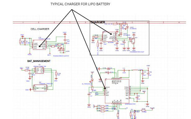
- Simple solution: Ideal diode combined with a TP4056 charger (low cost)
- Integrated solutions: ICs such as BQ24075, MAX77734, or TPS2116, which integrate load switching and power-path control
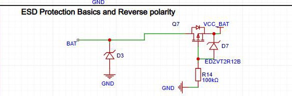
Battery connectors are a common source of accidental damage, especially in field-replaceable designs. Reverse polarity protection helps prevent catastrophic failure if a battery is connected incorrectly.
- Diode protection: Simple implementation, but introduces a voltage drop of about 0.3–0.7 V, which wastes energy.
- P-channel MOSFET protection (recommended): Provides near-zero voltage drop and much higher efficiency.
A classic P-MOSFET reverse-protection circuit:
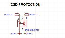
External connectors are common entry points for electrostatic discharge (ESD). USB ports, battery connectors, and exposed IO pins should always include protection.
Use bidirectional TVS diodes such as PESD5V0L1BA or SMAJ5.0CA, and place them as close as possible to the connector to intercept ESD events before they propagate into the PCB.
Turning an IoT concept into a reliable product involves far more than schematic design. Once wireless connectivity, battery operation, and real-world deployment are involved, PCB design quickly becomes a multidisciplinary challenge that touches RF engineering, power optimization, mechanical constraints, and large-scale manufacturing.
Many IoT projects encounter issues only after prototypes are built—unstable wireless performance, unexpected battery drain, EMC failures, or antenna efficiency problems caused by layout details. Addressing these challenges early in the design stage can significantly reduce development risk and shorten the path to production.
Bei PCBCool, we work with IoT developers to bridge the gap between design and manufacturing. Our team provides end-to-end IoT PCB support, including fabrication, RF-capable layout guidance, and full assembly services, helping ensure that IoT hardware designs are ready not only to function, but also to scale into reliable products.
If you’re developing a new IoT device—from low-power sensor nodes to connected industrial systems—PCBCool can help bring your design from prototype to production with confidence.