Unlike traditional circuit boards, flexible PCB are built on bendable dielectric substrates rather than rigid FR4. These circuits are typically very thin, with a total thickness ranging from 0.1 mm to 0.3 mm, which allows them to fit into tight spaces and endure repeated bending.
Like rigid PCB, flexible circuits can be manufactured as single-sided, double-sided, or multilayer boards, with advanced designs reaching 10 layers or more. However, designing a flexible PCB requires more careful planning than designing a rigid board. Factors such as material selection, stack-up configuration, bend areas, and layout rules all play a critical role in ensuring long-term reliability.
This is the most common flex substrate and the go-to choice for high-performance applications. As a high-temperature polymer that can handle continuous operating temperatures up to 200–260°C (and short-term peaks up to 400°C). It’s extremely durable, with excellent chemical resistance, low moisture absorption, and high tensile strength.
A low-cost option that’s great for budget-sensitive projects like consumer electronics or simple wearables. PET is flexible and lightweight but has lower heat resistance (typically up to 100–150°C) and poorer dimensional stability under temperature changes. It’s less suitable for soldering or high-heat processes, as it can warp or degrade.
Other less common substrates include:
- Liquid Crystal Polymer (LCP): High-end alternative to PI for RF/microwave applications due to low dielectric loss and excellent signal integrity at high frequencies.
- Polyethylene Naphthalate (PEN): A middle-ground between PET and PI, with better heat resistance (up to 180°C) but higher cost.
The conductive traces that carry signals and power, comprising two types of materials:
- Rolled Annealed (RA) Copper: Preferred for dynamic flex because it’s ductile and can withstand repeated bending without cracking (up to millions of cycles). It’s made by rolling copper sheets, resulting in a smooth, uniform grain structure.
- Electrodeposited (ED) Copper: Cheaper and rougher, created by electroplating copper onto the substrate. It’s more brittle and prone to fatigue in bending areas, so it’s better for static flex or rigid sections.
Including solder mask and coverlay:
- Solder Mask: A liquid photoimageable (LPI) coating, like on rigid PCB. It’s thinner (10–30µm), cheaper, and easier for fine-pitch designs but less flexible and prone to cracking in dynamic areas. Use solder mask for non-bend regions or low-cost flex; coverlay for high-reliability flex.
- Coverlay: The flexible equivalent of a solder mask, made from polyimide or polyester film with adhesive. It’s punched or laser-cut to expose pads, then laminated on. Coverlay provides excellent insulation, chemical resistance, and flexibility—essential for protecting traces in bend areas. It’s thicker (25–125µm) and more durable than solder mask but harder to apply precisely.
When laminating substrates with copper, there are two main approaches:
- Adhesiveless Laminates: These use a direct bond between the substrate and copper (via casting or sputtering), eliminating the adhesive layer. Benefits include better flexibility, higher heat resistance (no adhesive to degrade), thinner overall profile, and improved reliability in dynamic applications. They’re preferred for multilayer flex or high-temp needs but are more expensive to manufacture.
- Adhesive Laminates: Use an acrylic or epoxy adhesive to bond copper to the substrate. Cheaper and easier to produce, but the adhesive can reduce flexibility, add thickness, and fail under repeated bending or high heat. Common in low-cost, single-layer designs.
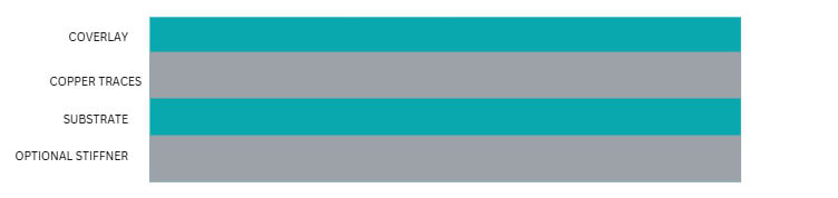
Simplest and cheapest; ideal for basic interconnects like LED strips or sensors.
Stackup:
- Coverlay (25 µm PI)
- Copper traces (18 µm RA)
- Substrate (50 µm PI, adhesiveless)
Total thickness: ~0.1 mm
Minimum bend radius: 3–5× thickness
Optional: stiffener on the bottom for mounting
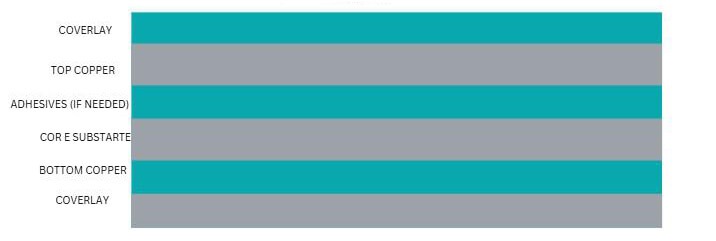
Adds a second copper layer for more complex routing; common in wearables or cameras.
Stackup:
- Coverlay (25 µm PI)
- Top copper (18 µm RA)
- Adhesive (optional, 25 µm)
- Core substrate (50 µm PI)
- Adhesive (25 µm)
- Bottom copper (18 µm RA)
- Coverlay (25 µm PI)
Total thickness: ~0.2mm
Supports plated through-holes (PTH) for interconnections.
Can handle dynamic flex if RA copper is used.
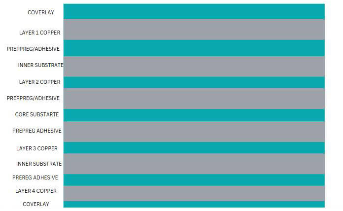
For high-density designs like foldable phones or medical devices; up to 12+ layers possible.
Stackup (4-layer):
- Coverlay (25 µm PI)
- Layer 1 copper (18 µm RA)
- Prepreg/adhesive (25 µm)
- Inner substrate (25 µm PI)
- Layer 2 copper (18 µm RA)
- Prepreg/adhesive (25 µm)
- Core substrate (50 µm PI)
- Prepreg/adhesive (25 µm)
- Layer 3 copper (18 µm RA)
- Inner substrate (25 µm PI)
- Prepreg/adhesive (25 µm)
- Layer 4 copper (18 µm RA)
- Coverlay (25 µm PI)
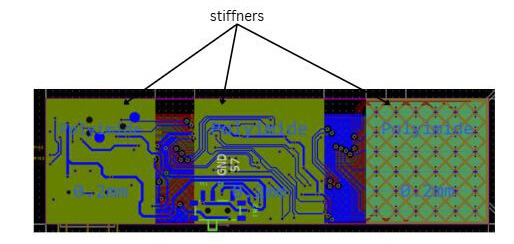
Additional details: Multiple stiffeners can be used—FR4 in rigid zones, PI in flexible zones
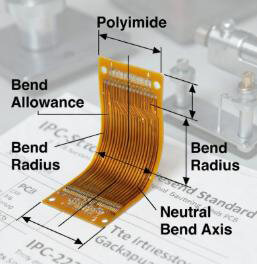
The bend radius is the smallest curve the flex PCB can be bent to without damage. It’s measured from the center of the curve to the inner surface of the flex.
Why it matters: Too tight a bend causes compression on the inner side and tension on the outer side, leading to copper fatigue, cracking, or substrate tearing.
Calculation formula: Minimum bend radius (R) is typically 3–10 times the flex thickness (T), depending on layers and bending type:
- Single-layer: R ≥ 3–6 × T
- Double-layer: R ≥ 6–10 × T
- Multilayer (3+): R ≥ 10–12 × T
Beispiel: For a 0.2mm thick double-layer flex, minimum R = 1.2–2.0mm.
Factors influencing it:
- Material: PI allows tighter radii than PET.
- Copper type: RA copper handles tighter bends than ED.
- Bend cycles: Reduce radius for static bends; increase for dynamic.
Static Bending: The flex is bent once or infrequently, like during assembly or installation (e.g., folding into a device housing).
- Allows tighter radii (e.g., 3× T for single-layer).
- Less stress on materials—focus on one-time formability.
- Common in cameras or wearables where the flex is shaped and stays put.
Dynamic Bending: Repeated flexing during use (e.g., folding phone hinges or robotic arms).
- Requires larger radii (e.g., 10× T or more) to survive 10,000–1,000,000+ cycles.
- Materials must be fatigue-resistant (RA copper, adhesiveless PI).
- Use IPC-TM-650 methods for cycle life.
Key difference: Static prioritizes space savings; dynamic emphasizes longevity. Mismatch can cause early failures—e.g., using static design in a drone’s vibrating arm.
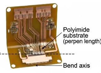
The bend axis is the line along which the flex folds, like the crease in paper.
Orientation rules: Align the bend axis perpendicular to the length of the flex for even stress distribution. Avoid skewing it at angles, as this creates uneven tension.
Best practices:
- Keep bends in a single plane (e.g., all horizontal or all vertical) to minimize twisting.
- For multiple bends, space them apart (at least 2–3× radius) to prevent stress concentration.
- In rigid-flex, ensure the flex section transitions smoothly to rigid areas without sharp angles.
Why it matters: Misaligned axes can cause “bookbinding” effects, where layers shift and delaminate.
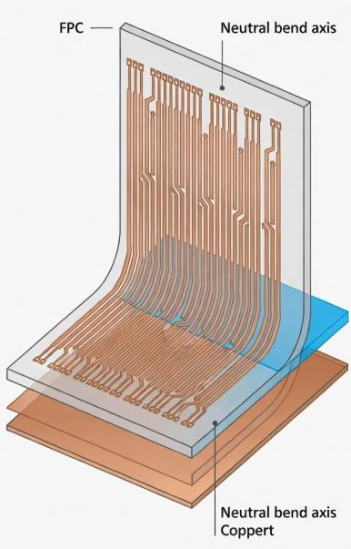
The neutral bend axis (or neutral plane) is an imaginary line through the flex cross-section where there’s zero strain during bending—no compression or tension.
How it works: In a symmetric stackup, it’s at the center. Asymmetries (e.g., thicker coverlay on one side) shift it.
Importance: Traces on the neutral axis experience the least stress, ideal for high-speed signals. Outer layers stretch/compress more, risking cracks.
Design tips:
- Balance the stackup (equal layers on both sides) to center the neutral axis.
- Place critical traces near the neutral axis.
- For dynamic bends, calculate shift: Neutral axis position = (Sum of layer thicknesses × their moduli) / total stiffness.
Analogy: Like the spine of a book—pages in the middle bend easily, outer ones stretch.
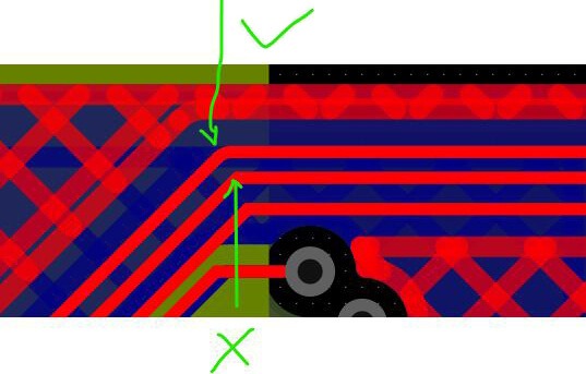
- Use curved traces instead of sharp corners: Sharp 90° corners create high stress concentrations during bending → copper can crack at the corner. → Always use rounded corners with a minimum radius of ~0.5–0.75 mm (often ≥ 0.030″ or ~0.75 mm per IPC-2223). Curved or filleted traces distribute stress evenly.
- Teardrops on pads: When a trace enters a pad or via, add a teardrop (tapered reinforcement) to prevent weak spots and cracking at the junction. Without teardrops, the abrupt width change creates a stress riser.
- Wider traces in bend areas (or tapered/staggered): Narrow traces are more prone to fatigue cracking in dynamic flex. → Increase trace width in bend zones (e.g., 1.5–2× normal width) or use tapered traces that gradually widen toward the bend. For multilayers: stagger traces between layers so no two traces align directly above each other in the bend → reduces cumulative stress.
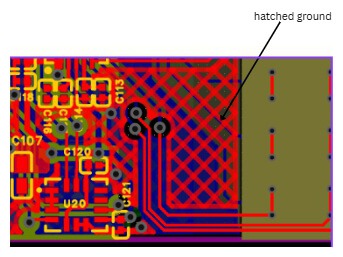
- Cross-hatched ground planes (instead of solid): Solid copper planes are too stiff and crack easily in flex areas. → Use a cross-hatched (grid/diamond) pattern in flex zones. Typical hatch: 45° or 60° angle, with line width ~0.1–0.2 mm and spacing 0.5–1 mm (adjust for impedance if needed). This maintains ~50% copper coverage for shielding/ground while allowing flexibility.
- Anchor spurs / tie-downs / anchors: Pads in flex areas need mechanical anchoring to prevent them from lifting or tearing during bending/coverlay application. → Add small copper spurs or “anchors” (like spider legs) extending from the pad into the coverlay area. These lock the pad to the substrate.
- Fillets: Add rounded fillets (concave curves) where traces meet pads or where coverlay meets pads. → Reduces stress risers and improves adhesion.
- Reinforced pads: Use larger annular rings or additional plating in high-stress pad areas. For SMT pads in flex: place them only on stiffened regions or use extra coverlay reinforcement.
- Avoid vias in bend zones (critical rule!): Vias are rigid and create stress concentrations → they often cause barrel cracks or delamination in dynamic flex. → Keep all vias outside bend areas (in rigid sections or stiffened islands in rigid-flex). If multilayer flex is unavoidable, place vias far from bends (at least 2–3× bend radius away).
- Use staggered vias if necessary: In multilayer flex (rare for pure dynamic flex), stagger vias between layers so they don’t stack directly. → Reduces localized stiffness and improves reliability. Still: best practice is no vias at all in flex regions.
Choose based on mechanical requirements and total stack thickness:
| Application / Need | Recommended Stiffener Thickness | Typical Material |
|---|
| Light SMT components, LEDs | 0.1–0.3 mm | PI or thin FR4 |
| Standard ZIF / FPC connectors | 0.4–0.8 mm | FR4 |
| Board-to-board connectors, heavy ICs | 0.8–1.2 mm | FR4 |
| High-vibration / shock resistance | 0.3–0.5 mm | Stainless steel |
| Ultra-thin wearable designs | 0.125–0.25 mm | PI |
Faustregel: Stiffener should make the total thickness in that area ~0.8–1.6 mm for good SMT/component support, but never exceed your mechanical envelope.
Stiffeners are bonded using adhesive:
Most common: Acrylic or epoxy-based pressure-sensitive adhesive (PSA) films (e.g., 3M 9077, DuPont Pyralux)
Dicke: Usually 25–50 µm per side
Types:
- Pre-applied PSA (easiest for prototyping)
- Thermoset adhesive (better long-term reliability, used in production)
Key points:
- Adhesive must cover the entire stiffener area (no voids)
- In rigid-flex, often use the same adhesive as coverlay bonding
- Heat + pressure during lamination (avoid bubbles/delamination)
- Place stiffeners only under components/connectors — never in dynamic bend zones
- Keep stiffener edge at least 1–2 mm away from bend area (transition zone)
- Overlap flex/coverlay by ~1–2 mm for good adhesion and stress relief
- Use rounded corners on stiffeners (radius ≥ 1 mm) to avoid stress risers
- For connectors: Stiffener should extend beyond connector body by 1–2 mm on all sides
- In rigid-flex, stiffeners often form part of the rigid section
- If multiple stiffeners are used, space them to avoid creating weak flex “hinges” between them
- If needed drill holes/vias, place them only in stiffened areas
Always submit your design files early for DFM review from your fabricator—they’ll flag issues and suggest cost-saving tweaks (e.g., relax tolerances where possible). Following IPC-2223 and IPC-6013 standards helps hit the sweet spot between performance and manufacturability.
Flex PCB are significantly more expensive (often 3–10× higher than equivalent rigid boards) due to several manufacturing and material factors:
- Specialized Materials: Polyimide (Kapton) substrates, adhesiveless laminates, and RA copper cost 3–8× more than FR-4. PET is cheaper but limited to low-performance apps.
- Complex Processes: Extra steps like precise coverlay lamination, windowing/punching, controlled impedance etching, and multiple cleaning/inspection cycles. Laser processing for fine features or microvias adds cost.
- Lower Yields: Thin materials are prone to defects (wrinkles, delamination, alignment errors). Scrap rates are higher, especially for dynamic flex or multilayers.
- Handling & Equipment: Requires cleanrooms, specialized fixtures, and slower processing to avoid damage. Rigid lines can’t handle flex without modifications.
- Low Volume / Customization: Flex designs are often low-to-medium volume with high customization (bend areas, stiffeners), reducing economies of scale.
- Testing & Qualification: More rigorous flex-cycle, thermal shock, and adhesion testing (per IPC-6013) increases cost.
Flexible PCB open up design possibilities that rigid boards simply cannot match—from wearable devices to foldable phones and compact industrial electronics. However, achieving reliable and high-performance flex circuits requires careful attention to materials, stack-up, bend radius, trace layout, stiffeners, and manufacturing constraints. Every detail matters: a small mistake in bend zones or pad design can compromise the entire board’s durability.
Bei PCBCool, we turn complex flexible PCB designs into reliable products. Our team excels in every stage of the process—design, manufacturing, and assembly—ensuring your flex projects meet both technical and practical requirements.
We can produce boards from single-layer to 6 layers, with board thicknesses ranging from 0.037 mm to 4 mm and tight tolerances of ±0.03 mm, as well as minimum hole diameters down to 0.10 mm.
Whether your design involves dynamic flexing, high-density routing, or rigid-flex combinations, we have the expertise and equipment to deliver consistently high-quality results.