Designing electronics for medical devices is significantly different from designing for consumer or industrial products. In medical applications, a PCB often becomes a critical part of a system that can directly impact patient safety. This makes every design decision—whether related to performance, reliability, or regulatory compliance—crucial.
As a result, medical PCB design demands a higher level of engineering discipline, encompassing system architecture, layout, component selection, and long-term reliability planning. In this article, we explore key design practices commonly applied in the development of PCB for modern medical devices.
Hospitals are full of electromagnetic activity from numerous sources:
- MRI scanners producing strong DC currents, gradient fields, and RF signals (64–128 MHz)
- X-ray and diathermy equipment operating around 27 MHz
- Wireless networks such as Wi-Fi and Bluetooth (2.4/5 GHz)
- Everyday devices, including mobile phones, and power-line hum (50/60 Hz)
This creates a complex electromagnetic environment. At the same time, medical devices often rely on extremely sensitive bio-signals—like ECG and EEG measurements in the microvolt range—which can be easily distorted or masked. Even minor interference can lead to false alarms, misdiagnoses, or malfunctions in life-critical equipment.
To protect patients and ensure device reliability, medical electronics must comply with strict standards. For instance, IEC 60601-1-2 sets limits on electromagnetic immunity and emissions, ensuring devices remain safe and functional even in busy hospital environments.
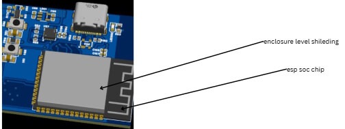
- Enclose sensitive PCB sections or the entire device in conductive metal (aluminum or copper) to block external RF and magnetic fields.
- Use EMI gaskets, honeycomb vents (for cooling), and shielded windows to allow airflow while blocking electromagnetic waves.
- MRI compatibility: Avoid ferromagnetic materials; use non-magnetic shielding to prevent image artifacts or device heating.
- Apply metal cans or covers over noisy digital sections to isolate them from analog bio-sensor areas.
- Use ground vias to stitch shielding cans to the ground plane, creating effective RF barriers.
- Use braided or foil-shielded cables for patient leads (ECG/EEG), grounding at a single end to prevent ground loops.
- Apply ferrite sleeves on cables to suppress common-mode noise from nearby hospital equipment.
- Filter RF signals from Wi-Fi, mobile phones, or MRI RF pulses while allowing DC and low-frequency bio-signals to pass.
- Place ferrite beads on power lines, signal paths, and I/O lines to act as high-frequency chokes (high impedance above ~100 MHz, low DC resistance).
- Placement tips: Close to the noise source (e.g., MCU power pin) or entry point (e.g., connector); combine with bypass capacitors for pi-filter configurations.
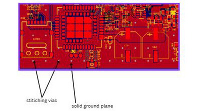
- Dedicate a solid (or nearly solid) ground plane in multilayer PCB for low-impedance return paths, minimizing loop areas that pick up EMI.
- Use stitching vias densely along edges and around sensitive areas to connect ground planes and reduce slot-antenna effects.
- Split analog and digital grounds if needed, but connect at a single point (star grounding) to prevent noise coupling.
- For EEG/ECG circuits: Minimize ground bounce from digital switching and use guard traces around high-impedance inputs.
- Notch filters at 50/60 Hz to remove common power-line interference in hospitals.
- Low-pass or band-stop filters targeting MRI RF (64–128 MHz) or diathermy (27 MHz).
- Common-mode chokes on differential pairs (e.g., ECG leads) to reject balanced hospital noise.
- Pi-filters (capacitor–inductor–capacitor) or ferrite + capacitor combinations on power inputs for broad-spectrum suppression.
In medical PCB design, reliability goes beyond technical performance—it directly impacts patient safety. For example, implantable devices must fail gracefully rather than abruptly, minimizing risk if a malfunction occurs.
To meet these stringent demands, medical devices—such as pacemakers and ventilators—are engineered for extremely high reliability, often targeting failure rates below 10^-6 per hour.
Achieving this level of safety requires systematic risk management in accordance with ISO 14971, which guides manufacturers in identifying hazards and implementing appropriate controls.
- Implement parallel, identical circuits (e.g., two processors in pacemakers) so that one can take over if the primary fails, monitored by voting logic or switchover mechanisms.
- On PCB, use isolated power domains and cross-checking signals to detect discrepancies.
Example: Implantable cardioverter-defibrillators (ICDs) use redundant sensing circuits to ensure accurate heart rhythm detection and reduce false shocks.
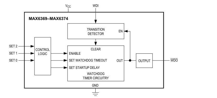
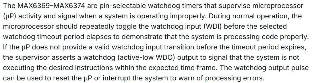
- Independent timers that reset the system if software becomes unresponsive (e.g., no “kick” signal received within a timeout).
- For medical PCB, use hardware-based watchdogs (e.g., MAX6369 IC) with adjustable timeouts ranging from milliseconds to seconds, addressing radiation-induced or environmental errors.
Application in pacemakers: Prevents firmware lockups, ensuring continuous pacing.
- Basic formula: MTBF = Total operating time / Number of failures
- For medical devices, an exponential distribution is often used: MTBF = 1 / λ (failure rate)
Consider mission time (e.g., 10 years for implants) and environmental stresses. Using MIL-HDBK-217, calculate λ based on component temperature, voltage, and quality level.
Simulates years of operation in weeks by applying elevated stresses such as temperature, humidity, and vibration, following standards like IEC 60601-1 Clause 15.
- Thermal acceleration: Arrhenius model with activation energy ~0.8 eV.
- HALT (Highly Accelerated Life Test): Pushes components to failure limits.
For medical applications: Include biocompatibility checks and test under simulated body conditions (37 °C, saline).
Process: Ramp stresses, monitor failures, and extrapolate normal-use lifetimes via Weibull analysis.
Top-down approach mapping undesired events (e.g., “pacemaker failure”) to root causes using logic gates (AND/OR).
In medical applications, FTA is integrated with FMEA per ISO 14971 to quantify risk probabilities.
Steps:
- Define top event
- Build tree with basic events
- Calculate minimal cut sets
- Assign probabilities (e.g., component failure rates)
Example: For EEG monitors, FTA might show “signal loss” due to OR (battery fail AND connector break), guiding redundancy improvements.
- Combine multiple mechanisms: dual circuits with watchdog timers, validated by MTBF, ALT, and FTA.
- PCB design tips: Use fault-tolerant layouts (e.g., mirrored traces) and select high-reliability components (e.g., MIL-spec capacitors).
Case study: Modern pacemakers achieve 99.999% uptime through triple redundancy in pacing logic, tested under ALT to simulate 15+ years of operation.
Medical PCB often handle sensitive patient information, such as vital signs, glucose readings, or cardiac data. Any data breach could compromise patient safety or lead to identity theft. Designers must implement security measures at both hardware and software levels, including encryption, access controls, and multi-factor authentication (MFA), to ensure the confidentiality, integrity, and availability of patient data.
These measures also help comply with regulations such as HIPAA (U.S., for protected health information, PHI) and GDPR (EU, for all personal data). Recent updates to HIPAA in 2026 make encryption and MFA mandatory. Noncompliance can result in substantial penalties—up to $1.5 million per incident under HIPAA or €20 million / 4% of global revenue under GDPR.
Use dedicated AES (Advanced Encryption Standard) hardware modules—such as TPM chips like Infineon OPTIGA or Atmel ATECC—directly on the PCB to encrypt data at rest and in transit.
- Secure bootloaders verify firmware signatures using cryptographic keys stored in secure elements (e.g., via ECDSA or RSA) before execution, preventing malware injection.
- Process: A root-of-trust in immutable ROM checks the bootloader, which then validates the OS and application software. This chain-of-trust ensures that only authorized code runs.
Medical application: In pacemakers or insulin pumps, secure bootloaders prevent tampering that could alter therapy dosing, while satisfying GDPR integrity requirements.
BLE (Bluetooth Low Energy) is commonly used for low-power connectivity in wearable medical devices. Security should include PIN or out-of-band (OOB) pairing and LE Secure Connections using AES-CCM encryption.
Best practices:
- Prefer Numeric Comparison pairing for medical devices rather than “Just Works,” which is less secure.
- Use GATT over secure links to protect sensitive data, such as glucose measurements.
Enhancements: Integrate with medical interoperability standards like IEEE 11073. Many modern devices—such as continuous glucose monitors (CGMs) like Dexcom—use encrypted BLE links to transmit data to apps, preventing eavesdropping.
The AFE must provide:
- High input impedance (>10 MΩ)
- Ultra-low noise (<1 µVrms)
- High common-mode rejection ratio (CMRR) (>110 dB)
- Programmable gain
Typical signal chain:
Instrumentation amplifier → High-pass filter (0.05–0.5 Hz to remove DC offset) → Programmable gain amplifier → Low-pass/anti-aliasing filter → Multiplexer → ADC
Medical-grade examples: Texas Instruments ADS129x family, Analog Devices AD8232/ADuCM355, or custom ASICs.
For glucose or pH sensors, use a transimpedance amplifier (TIA) to convert the nA–µA current from enzyme reactions into voltage.
- Resolution: 16–24 bits (effective 18–20 bits after noise filtering)
- Key specs: Low INL/DNL (<1 LSB), low noise (ENOB > 18), simultaneous multi-channel sampling (e.g., ECG + respiration)
- Preferred types: Sigma-Delta ADCs for oversampling and digital filtering (e.g., AD7175, ADS131M08)
- Integration tip: Place the ADC as close as possible to sensor pins to minimize trace inductance and pickup noise.
Hardware Techniques:
- Driven-Right-Leg (DRL) circuit for ECG/EEG to actively cancel common-mode 50/60 Hz noise
- Chopper-stabilized or auto-zero amplifiers to eliminate 1/f noise
- PCB layout strategies: Guard rings, Kelvin connections, star grounding
Analog Filtering:
- ECG: 0.5–40 Hz bandpass
- EEG: 0.05–10 Hz
- Glucose current: 0.1–5 Hz
Digital Filtering:
- FIR/IIR notch filters at 50/60 Hz
- Adaptive filters, wavelet denoising
Motion Artifact Reduction:
- Use 3-axis MEMS accelerometer data to feed adaptive noise cancellation algorithms, improving signal quality in dynamic environments
Designing medical PCB is a complex, multidisciplinary challenge. From EMI mitigation and reliability engineering to data security and precision sensor integration, every decision directly impacts patient safety and device performance. Achieving clinical-grade accuracy while ensuring compliance with strict regulatory standards requires careful planning, robust engineering, and deep expertise across electronics, firmware, and system integration.
Bei PCBCool, we provide a complete medical PCB solution. Our services cover the entire lifecycle:
- Design consulting: System architecture, PCB layout, component selection, and signal integrity optimization
- Precision manufacturing: High-reliability PCB fabrication using medical-grade materials and processes
- PCBA and full assembly: From analog front-ends to digital processing boards, including complete device assembly for wearables, implants, and diagnostic equipment
- Testing and validation: Functional testing, accelerated life testing, EMI/EMC compliance, and clinical-grade quality assurance
Partnering with PCBCool means you don’t just get a PCB—you get a trusted, end-to-end solution that meets the demanding requirements of modern medical devices, helping you bring safe, reliable, and high-performance products to market faster.