Grounding is one of the most misunderstood aspects of electronics, especially for beginners. Many designers focus their efforts on selecting components, drawing neat schematics, and routing signal traces, while giving little thought to how current actually flows through the ground network. On a real PCB, ground is not an ideal zero-volt node but a physical conductor with resistance and inductance, carrying real, time-varying currents.
Ignoring ground current flow can lead to frustrating problems: sensor readings become noisy, ADC values fluctuate unpredictably, audio circuits develop hum or buzz, microcontrollers reset or behave erratically, and systems may work only intermittently.
This tutorial focuses on PCB star grounding, one of the most practical techniques for small, low-frequency, mixed-signal. The explanations are structured so that beginners can follow the logic step by step, while intermediate designers gain a deeper understanding of why ground behaves the way it does in real hardware.
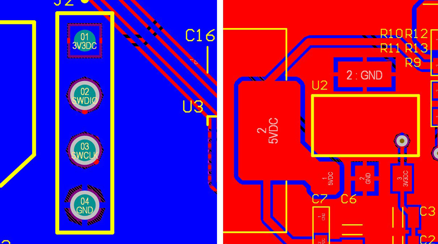
At its core, star grounding is a single-point grounding strategy. In this approach, each major return current path in the circuit is routed to a single physical location on the PCB, called the star point, which serves as the common reference for the entire system.
Instead of letting ground currents from different parts of the circuit mix freely, star grounding keeps them separated until they reach the star point. Circuits are typically divided into functional sections—analog, digital, and power—each with its own dedicated ground trace. These traces remain separate and converge only at the star point, minimizing interference between sections.
Electrically, star grounding helps ensure that:
- Noisy digital or power return currents do not flow through sensitive analog ground paths.
- Voltage drops caused by one section’s currents do not shift the ground reference of another section.
- The ground reference remains as stable and predictable as possible for critical measurements.
A helpful way to understand star grounding is to think of electrical current like water flowing through pipes. Imagine a system where water from different sources is allowed to drain into random locations. The pressure becomes unpredictable—some areas experience surges, others drops—and the overall system behavior is difficult to control.
Now consider a different setup: each pipe is routed carefully to a single, well-designed drain. Every flow has a clear, independent path to the same endpoint. Even if one pipe suddenly carries more water, the disturbance does not spread uncontrollably through the network, and pressure remains stable throughout.
Ground currents in a PCB behave similarly. Each part of a circuit draws current that must return through the ground. If multiple circuits share ground paths arbitrarily, the returning currents interfere with one another, causing voltage fluctuations along the ground. These fluctuations appear as noise, offsets, or instability in sensitive parts of the circuit.
Star grounding applies this “single drain” principle to electronics. Each major section of the circuit—analog, digital, or power—has its own return path to a central ground point. This ensures ground currents do not flow through unintended areas and keeps the ground reference stable and predictable.
This mental model highlights the essence of star grounding: it is not about symmetry or neat PCB layout, but about directing current flow so that interactions are minimized and circuit behavior remains reliable.
This analogy is most accurate for low-frequency or mixed-signal circuits. At high frequencies, parasitic inductance and capacitance may introduce additional effects on current flow.
In textbooks, ground is often shown as 0 V. In real PCB, however, ground is a physical conductor that:
- Has resistance
- Has inductance
- Carries current
Whenever current flows through resistance, it generates a voltage drop:
V = I × R
As a result, the ground voltage changes along its path. These variations are commonly referred to as:
- Ground noise
- Ground bounce
- Ground offset
Digital ICs switch thousands or millions of times per second. They draw current in short, sharp bursts, creating high di/dt spikes.
If analog circuits share the same ground path:
- Their “ground reference” shifts
- Small signals can be corrupted
- ADC readings may jump
- Audio circuits can develop buzz or hum
- Controlling where ground current flows
- Preventing digital return currents from crossing analog ground paths
- Keeping sensitive references stable
This approach is particularly effective in:
- Sensor boards
- Audio circuits
- Medical electronics
- Small IoT devices
Star grounding works best when all three of the following conditions are met:
Small PCB Size
- Short traces help reduce inductance and resistance, making current paths more predictable.
Low Frequency (≤ 1 MHz)
- At low frequencies, long return paths are tolerable, signal reflections are minimal, and lumped-element assumptions remain valid.
Mixed-Signal Design
Boards that combine analog, digital, and power sections benefit most. Typical examples include:
- Temperature sensor + microcontroller
- Heart-rate monitor
- Load cell + ADC + microcontroller
- Audio preamplifier + digital control
Star grounding becomes less effective when:
- PCB size is large
- Frequencies are high (>10 MHz)
- Fast edge signals dominate (USB, Ethernet, RF)
- Return paths must closely follow signal paths
In these cases, designers often rely on:
- Continuous ground planes
- Hybrid grounding strategies
The star point is the central reference for all ground currents. It should be:
- Low impedance
- Mechanically robust
- Electrically quiet (free from interference)
Common ways to implement the star point include:
- A large copper pad
- A solid copper pour
- Power connector ground pin
- Voltage regulator ground pad
To control current flow, the board is typically divided into:
- Analog Ground (AGND)
- Digital Ground (DGND)
- Power Ground (PGND)
These domains are conceptual—routing disciplines rather than physically isolated islands—and they meet only once at the star point.
Each domain should have its own trace that goes directly to the star point, without sharing return paths.
This approach prevents:
- Ground loops
- Noise injection
- Uncontrolled current flow
Before any routing begins, first classify each circuit block by how it draws current and how sensitive it is to noise. Ask yourself:
- Which parts draw pulsed or switching current?
- Which parts require a quiet, stable reference?
A typical classification looks like this:
- MCU → Digital (noisy)
- Switching regulator → Power (very noisy)
- Sensor / ADC → Analog (very sensitive)
The star point should be located where ground currents naturally converge and where impedance can be kept low.
Good locations include:
- Near the power entry
- Near the voltage regulator ground
- Near bulk decoupling capacitors (high-current return paths)
Avoid placing the star point:
- At board edges far from loads
- Behind thin or long trace connections
- At the end of daisy-chained ground paths
Analog ground is the most sensitive and should be routed before anything else.
Basic rules for analog ground routing:
- Keep it short
- Make it wide (≥ 1 mm is a reasonable guideline)
- Avoid digital crossings
- Avoid vias if possible
Warum dies wichtig ist:
Analog signals are often measured in microvolts or millivolts. Even very small ground voltage shifts can introduce significant measurement error or noise.
Digital ground is less sensitive, but it is noisier.
Digital ground traces:
- Can be narrower than analog ground
- Should still be short
- Must route directly to the star point
Never allow digital ground to:
- Pass under analog components
- Share any trace segment with analog ground
Power ground carries the highest currents and demands special care.
Power ground:
- Must be thick and low impedance
- Should connect near bulk and local decoupling capacitors
- Must provide a local return path for switching currents
As a final verification step, confirm that:
- All ground domains connect at one and only one point
- There are no accidental copper bridges
- Polygon pours or auto-fills have not created hidden connections
Scenario:
- Temperature sensor (analog)
- 12-bit ADC
- Microcontroller
- Battery powered
Correct star grounding strategy:
- Sensor ground → wide analog trace → star point
- ADC reference ground → same analog trace
- MCU ground → separate digital trace → star point
- Battery negative → directly to star point
Ergebnis:
- Stable ADC readings
- No conversion jitter
- No temperature drift caused by MCU activity