IoT Industry
- 4+N+4 HDI, 64μm/64μm Min Trace Width/Spacing, Fine-Pitch PCB
- MLF, QFP, CSP, WLCSP, Flip-Chip Small Package Solutions
- Low-Power, Connectivity, and System Stability Optimization
20+ Years of Experience in the IoT Industry
With over 20 years in the electronic manufacturing industry, PCBCool has built a solid foundation in delivering tailored solutions for the IoT sector.
Our expertise spans from simple ESP32-based projects to high-precision PCBs, covering a wide range of applications from smart home devices to industrial automation systems.
We provide comprehensive manufacturing services and structure our teams by industry specialization, ensuring that the members handling your projects possess extensive IoT experience.
Whether you’re working on prototypes or large-scale production, you can trust us to bring your PCB and PCBA projects to life with confidence.
IoT PCB Solutions We’ve Delivered
Smart Home Devices
- Smart Thermostats
- Home Security Systems
- Smart Lighting Controls
Wearable Technology
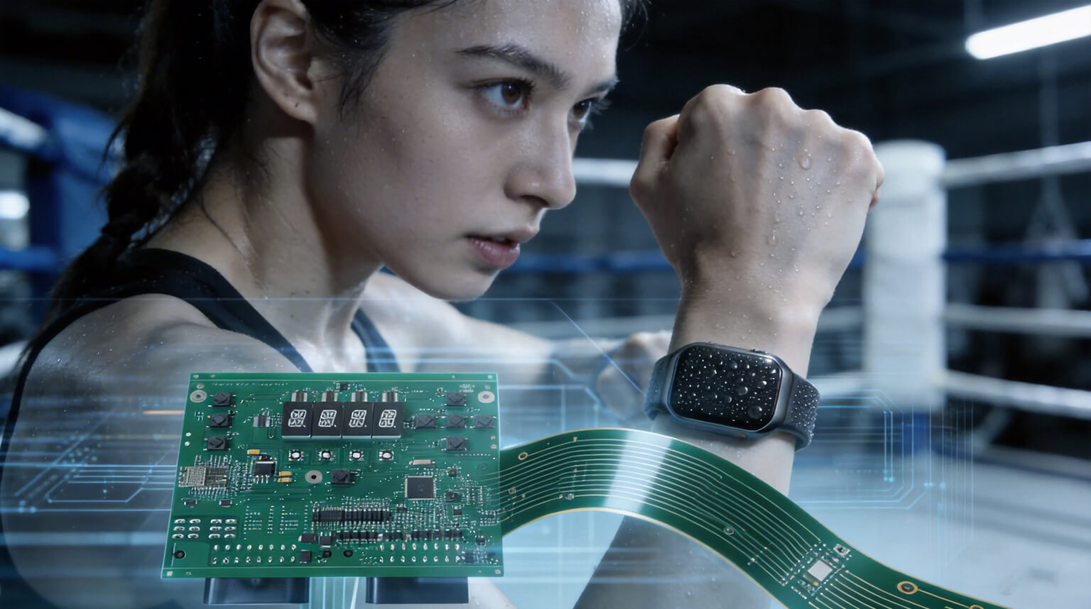
- Fitness Trackers
- Smart Watches
- Health Monitoring Devices
Industrial IoT (IIoT)
- Predictive Maintenance Sensors
- Remote Monitoring Systems
- Industrial Automation Controllers
Connected Vehicles
- Telematics Systems
- Fleet Management Solutions
- Vehicle Tracking Devices
Healthcare IoT
- Remote Patient Monitoring
- Medical Wearables
- Telehealth Devices
Smart Agriculture
- Precision Farming Sensors
- Crop Monitoring Systems
- Livestock Tracking Solutions
Smart Cities
- Traffic Management Systems
- Smart Parking Solutions
- Environmental Monitoring Devices
IoT for Energy Management
- Smart Grids
- Energy Metering Solutions
- Solar Panel Monitoring Systems
View Past Projects
Review our past projects to see how we addressed customers’ technical and manufacturing challenges.
Our Valued Clients
Manufacturing Compliance
Industry Certification Support
-
Support for ISO 9001 quality management system
-
Compliance with ISO 14001 environmental management system
-
Adherence to ISO 45001 occupational health and safety standards
-
Support for RoHS / REACH environmental compliance
-
IPC standards compliance: IPC-A-610, IPC J-STD-001
-
UL, CE, and other industry-specific standards and customer requirements
-
Compliance with ISO/IEC 30141 IoT Reference Architecture
-
OneM2M certification for IoT interoperability
-
Adherence to ITU-T Y.2060 Internet of Things framework
Production Process Control
-
Full BOM and lot traceability across production
-
Material traceability (components, boards, solder paste, etc.)
-
Process documentation for regulated manufacturing
-
First Article Inspection (FAI) support
-
In-process quality checks and monitoring
-
Controlled ESD & cleanroom processes (if applicable)
-
Complete inspection records and test reports
-
Change control and nonconformance management
End-to-End Solutions
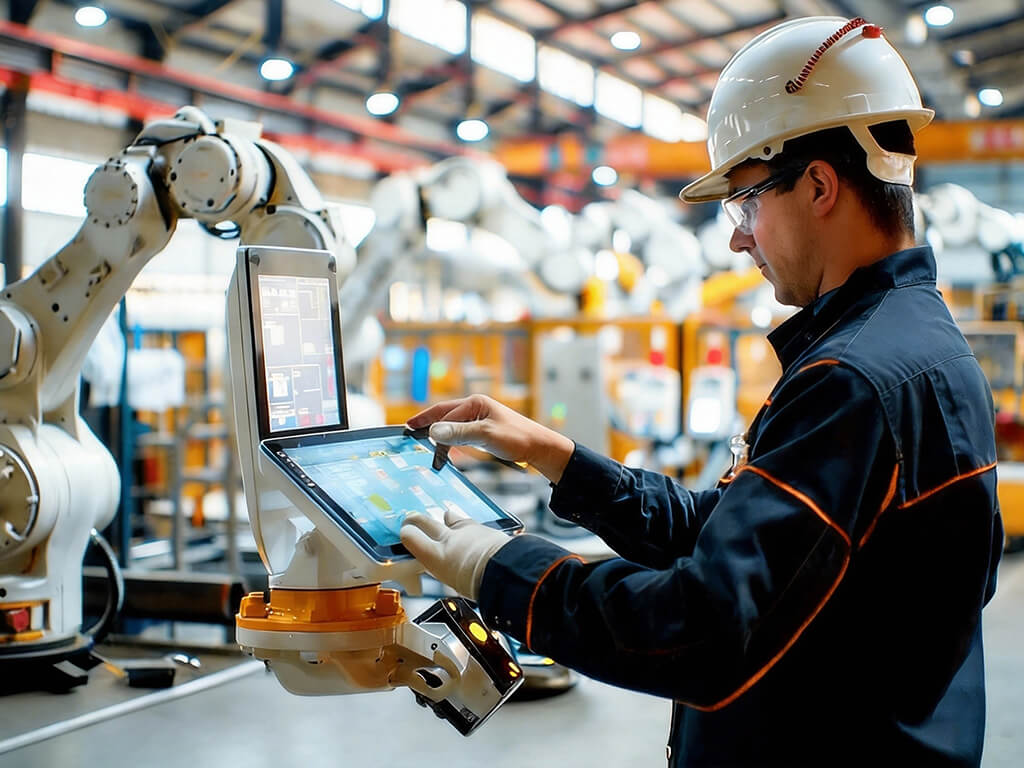
We provide complete end-to-end IoT device manufacturing, from PCB production to box build assembly. Our team of 177 engineers and R&D specialists ensures every project is optimized for cost-effectiveness and performance.
Cutting-Edge Technologies
Our automated facility features state-of-the-art equipment, including the JT1000 with 12-zone reflow soldering for stable assembly and the YSM20R, capable of placing up to 44,000 components per hour, including ultra-small 01005-sized parts.
Why IoT Device Manufacturers Choose PCBCool
Outsourcing IoT device manufacturing requires advanced connectivity, high data throughput, and power-efficient solutions.
When your devices demand precision in high-density PCBs, low-power design optimization, and real-time performance —
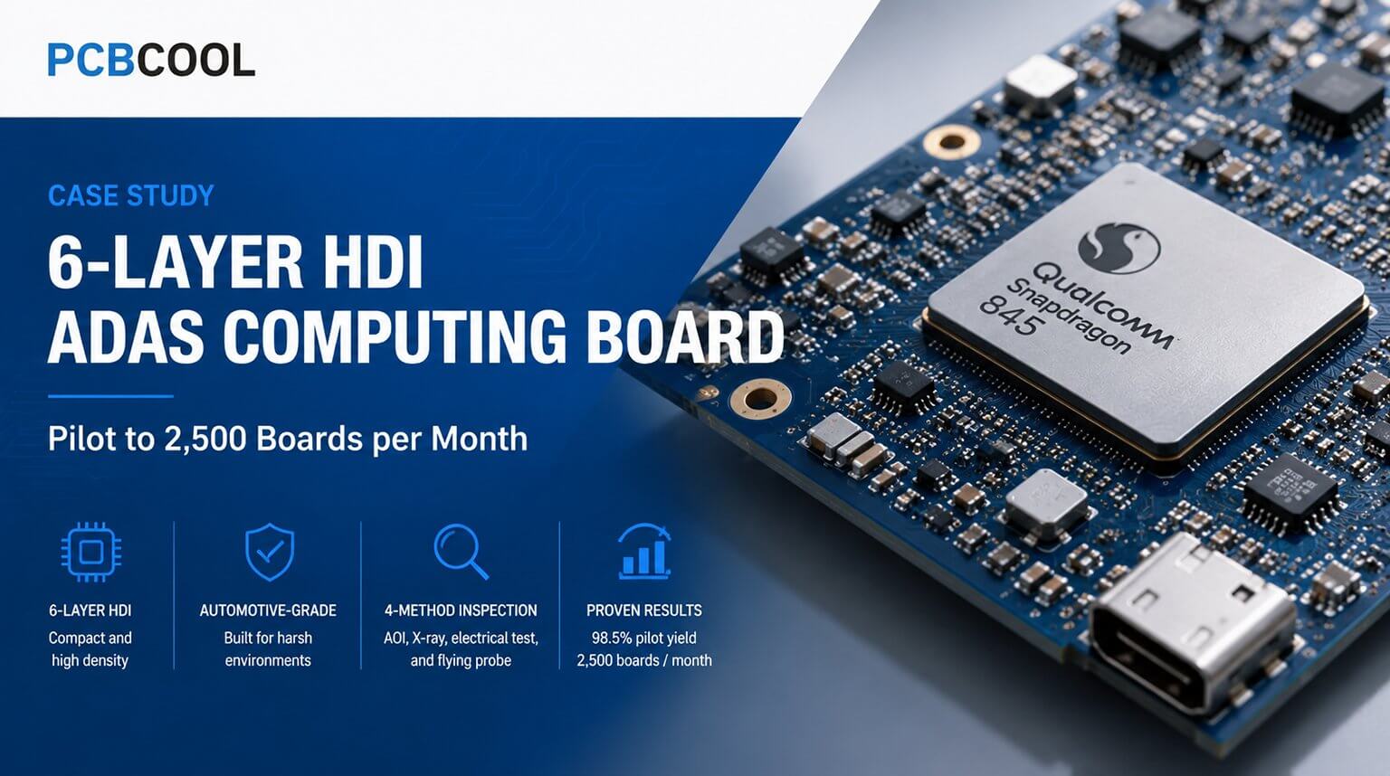
Case Studies
Frequently Asked Questions
A: We typically deliver IoT PCB prototypes within 3-7 days, depending on design complexity and requirements.
A: We can manufacture up to 40 layers for rigid boards and up to 6 layers for flexible boards, depending on substrate material.
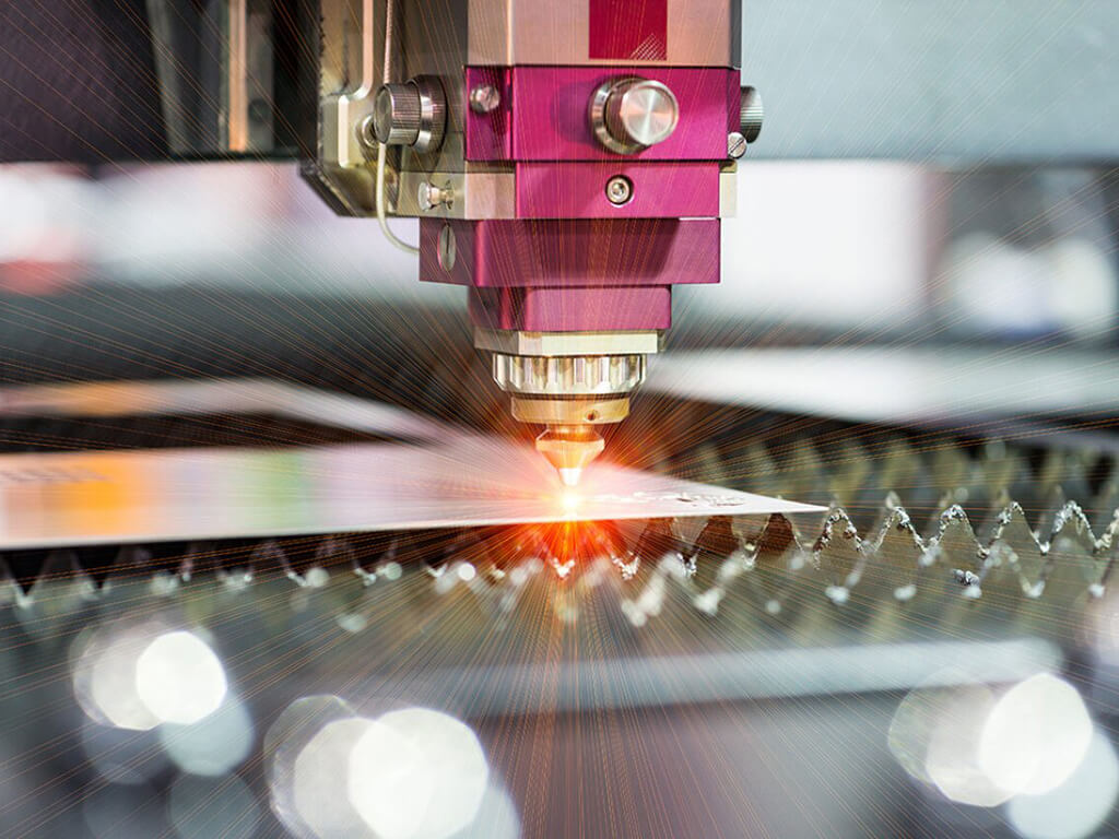
A: Yes, we use laser drilling for high-density applications that require smaller hole sizes and tighter spacing.
A: We use traditional FR4, high-frequency materials like Rogers for high-speed designs, and flexible substrates for wearables and micro IoT applications.
A: Yes, our engineering and R&D teams offer custom PCB design services for both standard and specialized IoT projects.
A: We use HDI (High-Density Interconnect) technology, multi-layer PCB designs, and laser drilling to optimize space usage.
A: Our engineering team optimizes trace width, component selection, and power distribution to achieve maximum energy efficiency.
A: We conduct electrical, functional, and thermal testing, among others, to ensure optimal performance.
A: Yes, we can integrate various wireless modules, including Wi-Fi, Bluetooth, Zigbee, LoRa, and more into your IoT designs.
A: Yes, we offer environmental testing, including temperature, humidity, and vibration testing, ensuring your IoT devices perform reliably in various conditions.
A: We maintain strong supplier relationships and use alternative sourcing strategies to ensure continuous production, even when components become obsolete.
A: Yes, we handle projects from prototype to large-scale production, with no minimum order quantity.
A: We offer ongoing support, including repairs, upgrades, and maintenance, with a dedicated account manager for continuous assistance.
A: We provide both manual and automated assembly services, including SMT, through-hole, and mixed-technology assembly.
A: You can specify preferred brands or authorized distributors, or use our supplier network for cost-effective and verified components.
A: Yes, we assist with obtaining regulatory certifications such as CE, UL, and RoHS, tailored to your specific requirements.
A: We lower costs through component alternatives (when possible), DFM/DFA checks to avoid production errors, and optimized sourcing strategies.
A: Simply contact us with your project details. Your dedicated account manager will reach out to discuss the next steps.