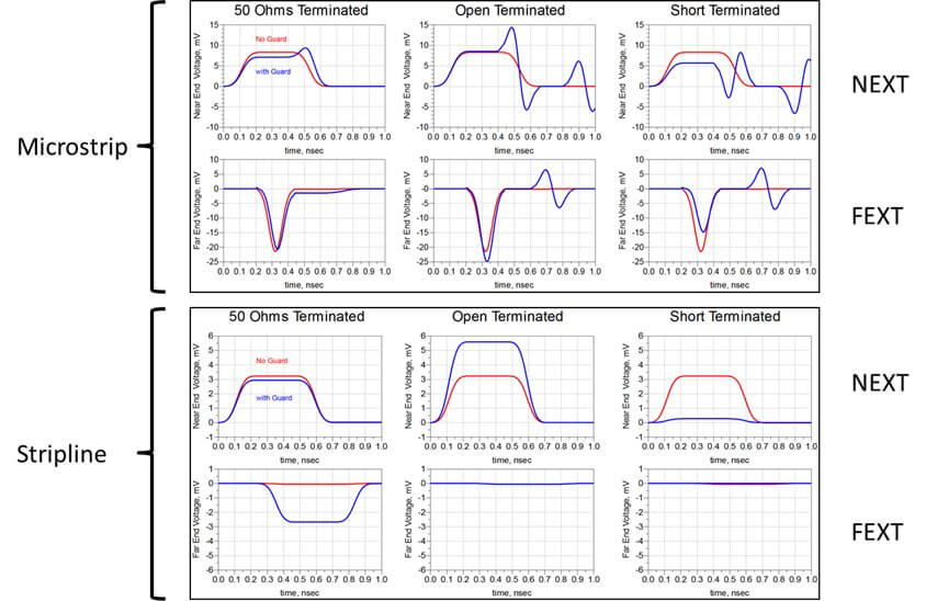
Wie man Übersprechen auf einer Leiterplatte reduziert
Erfahren Sie, wie Sie Übersprechen auf Leiterplatten mit praktischen Tipps zu Ursachen, Erkennung und Layout-Design reduzieren können, um Signalintegrität und Hochleistungsfähigkeit zu verbessern.

Verwandte Artikel

PCBCool 2026 Drachenbootfest – Feiertagshinweis und Dankeschön
Während des Drachenbootfestes 2026 werden die chinesischen Fabriken von PCBCool die Produktion einstellen, während die Projektteams für die Kundenbetreuung zur Verfügung stehen.
Die 7 Top-US-Leiterplattenhersteller, die man 2026 im Auge behalten sollte
Entdecken Sie, wie der US-amerikanische Leiterplattenmarkt High-End-Elektronik unterstützt, und sehen Sie sich die Liste von PCBCool mit 7 empfohlenen US-Leiterplattenherstellern für 2026 an.

6 Strategien für den Leiterplattenmaterial-Engpass 2026
Das Wachstum von KI-Servern verknappt das Angebot an hochwertigen Leiterplattenmaterialien, darunter Glasgewebe, Harz und CCL. PCBCool teilt 6 praktische Strategien, um Ihren Teams zu helfen, Materialrisiken und Lieferzeitdruck zu reduzieren.

GSR-fähiges Multi-Biomarker-Athletenmonitoring-Armband – Fallstudie
Sehen Sie, wie PS Electronics einem europäischen Sporttechnik-Startup geholfen hat, ein GSR-gestütztes Sportlerüberwachungsarmband in ein herstellbares Produkt zu verwandeln.
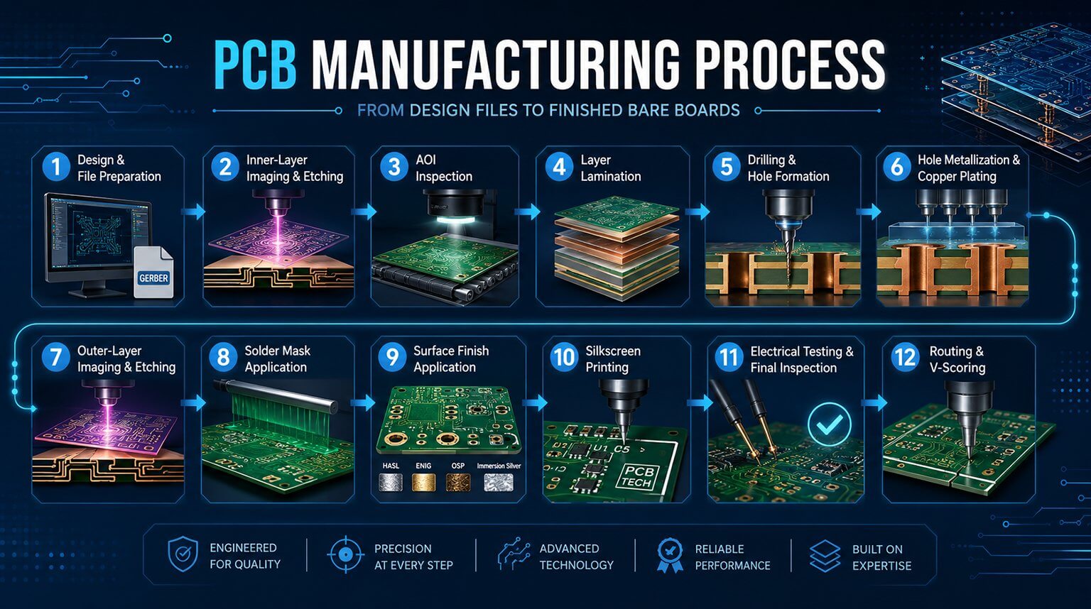
Wie eine Leiterplatte Schritt für Schritt hergestellt wird
PCBCool erklärt den Standardprozess der Herstellung von Leiterplatten ohne Oberflächenveredelung Schritt für Schritt anhand von Text, Bildern und Videos, von den Produktionsdateien bis zu den fertigen Leiterplatten.
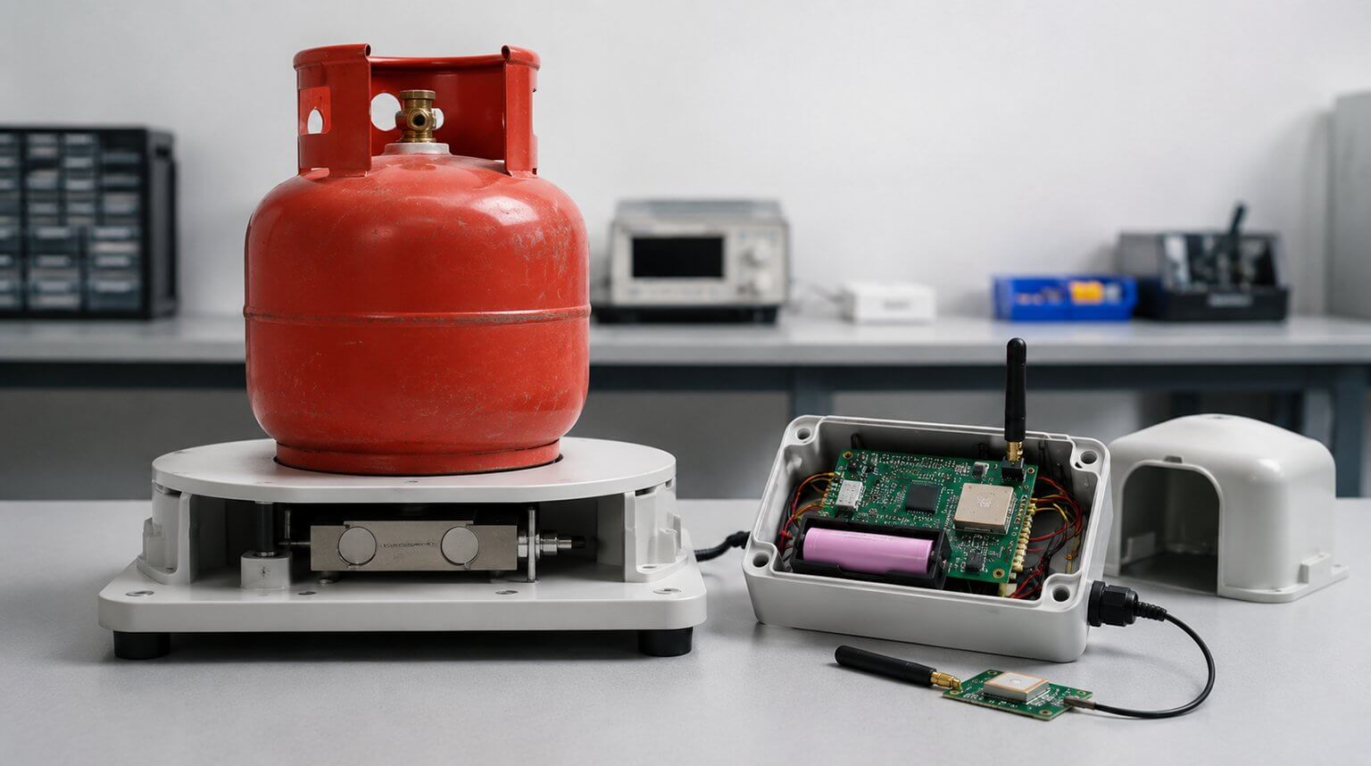
LPG-Gasmelder Mechanisch-Elektrisches Prototyp-Fallstudie
PS Electronics definierte einen mechanisch-elektrischen Prototypenpfad für ein intelligentes LPG-Gasanzeigen-Messgerät, das die Genauigkeit der Lastzelle, die Gehäusestruktur, die Batterieanordnung, die HF-Freiräume und die Produktionsreife berücksichtigte.
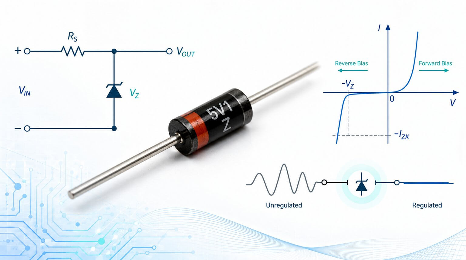
Alles, was Sie über Zener-Dioden wissen müssen
Eine Zener-Diode ist eine speziell dotierte pn-Übergangsdiode, die für den Betrieb im umgekehrten Durchbruch ausgelegt ist und eine stabile Spannung aufrechterhält.
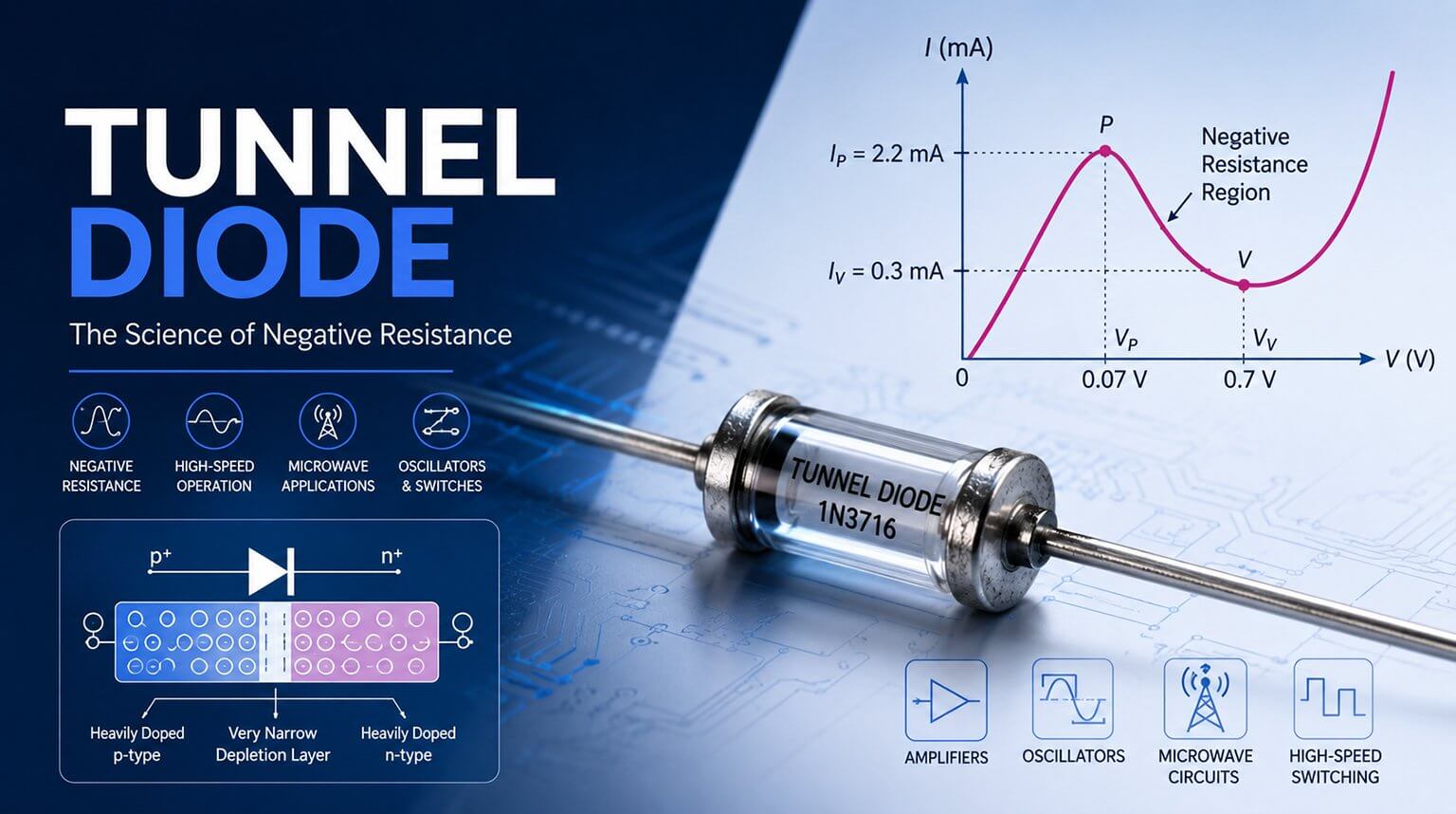
Umfassender Leitfaden zu Tunneldioden
Eine Tunneldiode ist eine stark dotierte p-n-Übergangsdiode, die durch Quantentunneln einen negativen Widerstand erzeugt. Diese Anleitung erklärt ihr Funktionsprinzip, ihre Eigenschaften und ihre Anwendungen.
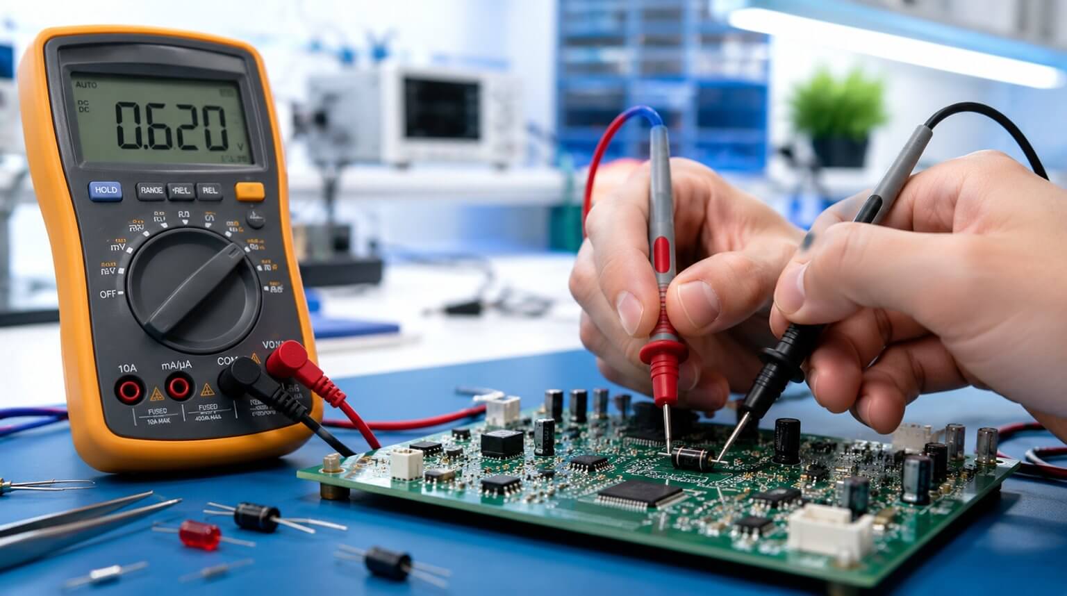
Wie man eine Diode testet, um festzustellen, ob sie defekt ist
Testen Sie eine Diode in Durchlass- und Sperrrichtung. Eine gute Diode zeigt einen normalen Durchlassspannungsabfall und sperrt den Strom in umgekehrter Richtung; anormale Werte deuten normalerweise auf eine defekte Diode hin.
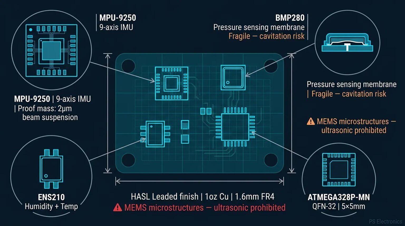
MEMS-Sensoren-PCBA-Ultraschallreinigung-Schadensfall-Fallstudie
Ein MEMS-Sensor-PCBA-Projekt litt nach der Ultraschallreinigung unter Sensorfehlern. Diese Fallstudie zeigt, wie PS Electronics den Prozess neu gestaltete, EOL-Komponenten verifizierte und zuverlässige Platinen ohne Sensorbeschädigung lieferte.
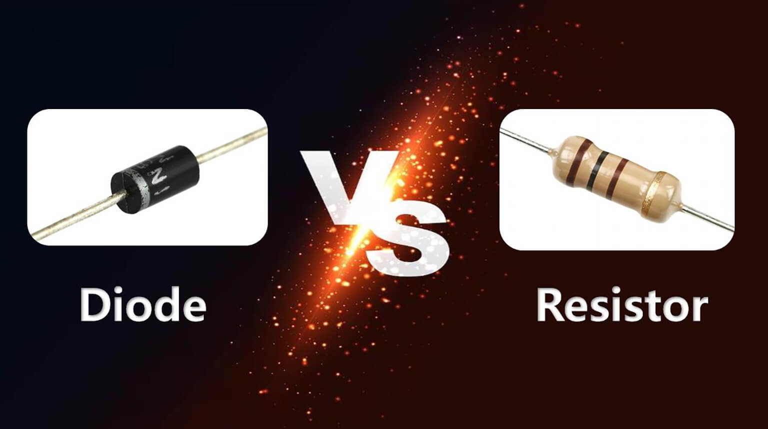
Der Unterschied zwischen Dioden und Widerständen
Eine Diode ist eine Halbleiterkomponente, die Strom hauptsächlich in einer Richtung fließen lässt, während ein Widerstand eine passive Komponente ist, die den Strom in einem Stromkreis begrenzt.
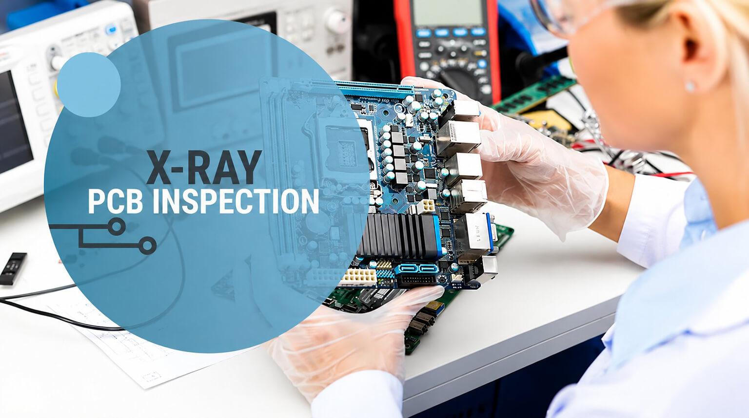
Was ist die PCB-Röntgeninspektion und warum ist sie notwendig?
Leiterplattenröntgeninspektion nutzt zerstörungsfreie Bildgebung zur Überprüfung verborgener Lötstellen und interner Leiterplattenstrukturen, insbesondere bei BGA-, QFN- und hochdichten SMT-Bestückungen, wo die Sichtprüfung nicht ausreicht.
