As the demand for signal speed and frequency in modern electronic devices continues to rise, PCB are moving towards higher density designs, with high-density interconnect (HDI) technology and multi-layer designs becoming a growing trend.
Given these trends, via design has gained increasing significance. It is not just essential for electrical connections; it also plays a key role in ensuring the signal integrity, manufacturability, and thermal performance of the circuit board.
Therefore, for modern electronic engineers and designers, it is crucial to understand how via geometry and manufacturing limitations affect routing decisions and layout reliability.
This guide will focus on how to properly handle vias in PCB design and layout, including how to choose via parameters, how to place vias correctly during routing, and the practical trade-offs to consider when designing 1-4 layer PCB and more complex multi-layer boards.
During PCB layout, vias are introduced when routing constraints require a trace to move to another layer. Designers typically begin routing on the outer layers and insert vias only when necessary to avoid congestion, maintain short trace lengths, or reach internal planes.
Every via consumes routing space, introduces parasitic effects, and adds fabrication cost. For this reason, experienced designers treat vias as controlled design elements rather than placing them automatically or excessively, whether they are through-hole, blind, buried, or microvias.
In practical layout work, through-hole vias are the default choice for most 1–4 layer PCB because they are universally supported by fabrication houses and require no special stackup planning. Designers typically pre-define one or two standard through-hole via sizes in the CAD tool and reuse them throughout the layout to maintain consistency and manufacturability. These standard vias are then applied consistently during interactive routing rather than adjusted on a per-net basis.
Despite their simplicity, through-hole vias present several critical constraints that engineers must account for in advanced PCB designs:
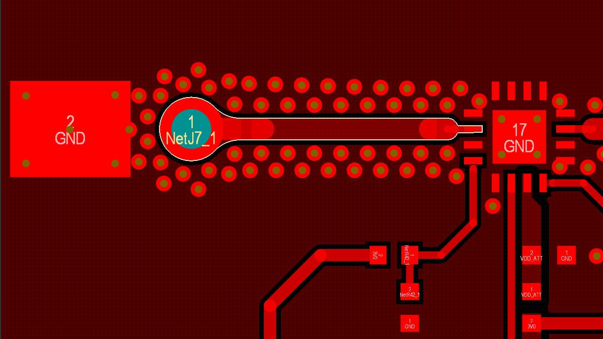
From a layout perspective, each through-hole via blocks routing channels on every layer, which is why designers often push it closer to component pads and avoid placing them in dense routing corridors. Through-hole vias occupy routing space on every layer of the PCB, even when the signal only transitions between two specific layers.
This significantly reduces the available “routing channels” on inner layers. One common mitigation strategy is Non-Functional Pad (NFP) removal, where the annular rings are “turned off” on layers where no track is connected to the via. While this reclaims some space, the physical hole and its associated clearance still remain an obstacle.
Before routing begins, PCB designers define via parameters based on fabrication limits and board requirements. These parameters include drill diameter, finished hole size, pad diameter, annular ring width, and antipad clearance.
For most low-cost 1–4 layer boards, designers select conservative values (for example, a 0.30 mm drill with a 0.60 mm pad) to maximize yield and avoid plating reliability issues. Aggressively small vias may reduce routing space but often increase fabrication risk and cost. For example, power and ground vias are often assigned larger drill sizes than signal vias to reduce resistance and improve current handling.
Once defined, these via sizes are locked into the design rules so vias placed during routing remain consistent across the entire board.
As layer counts increase, the total board thickness usually increases as well. Due to Aspect Ratio limitations (the ratio of board thickness to drill diameter), the via hole size must be increased to ensure the plating chemistry can effectively coat the center of the barrel.
As you increase the drill diameter, you must correspondingly increase the annular ring size to maintain mechanical integrity. Because the area occupied by a via increases by the square of its diameter, a slight increase in drill size for a thick, high-layer-count board results in a massive loss of routing density across the entire stackup.
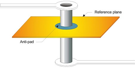
In high-speed designs, maintaining a continuous reference plane (usually Ground) is vital for impedance control. Through-hole vias require “clearance holes” or anti-pads in these copper planes.
When multiple through-hole vias are placed in a row (such as in a connector footprint or a bus), these circular voids can merge to create a large “slot” in the ground plane. This forces the return current to take a long path around the slot, increasing loop inductance and causing impedance mismatches. Designers often must “walk” traces around these large void areas, which complicates the layout and can degrade signal quality.
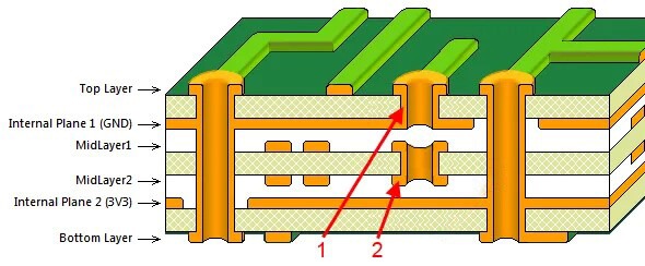
Perhaps the most significant drawback for high-frequency signals is the via stub. If a signal transitions from Layer 1 to Layer 3 in a 6-layer board, the portion of the via barrel extending from Layer 3 down to Layer 6 is electrically “extra.”
This unused portion acts as a resonant stub or an antenna. It introduces:
- Reflections: The signal “sees” the end of the stub and reflects back into the main trace.
- Parasitic Capacitance/Inductance: The extra copper adds unintended capacitance and inductance, which can shift the characteristic impedance of the transmission line.
- EMI: At Gigahertz frequencies, these stubs can radiate energy, leading to Electromagnetic Interference (EMI) issues. In extreme cases, these stubs must be removed via back-drilling, an additional manufacturing step that increases costs.
From a PCB design standpoint, blind and buried vias are introduced only when routing density or BGA escape requirements exceed what standard through-hole vias can support.
Both via types are used to significantly increase routing density by freeing up real estate on layers not involved in the connection. Unlike through-hole vias, these do not penetrate the entire stackup, allowing for traces to be routed directly above or below them on other layers.
- Blinde Leiterbahnen Connect an outer layer to one or more inner layers but do not exit the other side. For example, they can connect the top layer to any internal layer in a multilayer board but not the bottom layer. They are visible on only one end (either top or bottom), hence the name “blind” via.
- Vergrabene Vias Connect two or more inner layers and are completely encapsulated within the board. They can connect any combination of internal layers but cannot touch the top or bottom external layers. These are completely invisible from the outside of a finished PCB.
The primary drawback of blind and buried vias is the increased cost and manufacturing complexity. Because these vias do not go through the whole board, they cannot be drilled after the entire board is pressed together. Instead, they require sequential lamination cycles.
- Sequential Lamination: The manufacturer must drill and plate the specific internal layers first, laminate them together, and then potentially drill and plate again for the outer layers. Each “press” cycle adds high cost and increases the risk of layer registration errors.
- Drill Depth Control: Blind vias are often created using Controlled Depth Drilling (mechanical) or Laser Drilling. Mechanical depth control is difficult to calibrate perfectly; if the drill goes too deep, it may short to the layer below it.
- Aspect Ratio Sensitivities: Because blind vias are “dead-end” holes, they are much harder to plate than through-holes. Plating chemistry has difficulty circulating in a hole that has no exit. Therefore, the aspect ratio for blind vias is much stricter, typically 1:1, meaning the hole diameter must be at least as large as the depth of the hole.
From a signal integrity perspective, blind and buried vias are far superior to through-hole vias in high-frequency applications:
- Elimination of Vias Stubs: In our through-hole example, it was noted that the unused portion of a via acts as an antenna (a stub). Blind and buried vias completely eliminate the stub, as the copper barrel ends exactly where the signal transitions. This prevents signal reflections and resonance that can degrade data at high speeds.
- Plane Integrity: Since these vias do not penetrate all layers, they do not create “Swiss cheese” voids in every ground plane. This allows for much more consistent return paths and simplifies impedance-controlled routing, as the designer doesn’t have to “walk around” as many clearance voids on the internal layers.
- BGA Escape Routing: Blind vias are often essential for high-pin-count BGAs. They allow the designer to “drop” a signal from a BGA pad to an internal layer and then immediately route away, leaving the layers beneath it completely clear for other signals or power rails. Hence in a way they are essential for minimizing the layer count.
With HDI technology, the standard mechanical via reaches its physical and economic limits. This is where microvias become essential. IPC defines a microvia as a hole with an aspect ratio of 1:1 and a diameter typically ≤ 0.15mm (6 mil).
Unlike through-hole or buried vias, microvias are typically laser-drilled. This allows for extreme precision and a much smaller footprint. Because laser pulses can be controlled with high accuracy, they are used to drill through exactly one dielectric layer and stop at a target copper landing pad. This process is faster than mechanical drilling for small diameters and avoids the mechanical stresses and bit-breakage risks associated with tiny traditional drills.
The most critical engineering constraint for microvias is the Aspect Ratio. To ensure that the plating solution can effectively enter the hole and deposit a reliable copper layer, the aspect ratio is generally restricted to 1:1 or 0.75:1.
Aspect Ratio=Drill Depth / Drill Diameter
If the dielectric (Prepreg) is too thick for a given microvia diameter, the hole becomes a “deep well” that the plating chemistry cannot reach. This results in weak or voided copper at the base of the via, leading to intermittent connections or total failure during thermal expansion. Therefore, microvias are almost always restricted to spanning only one layer (e.g., L1 to L2).
When a signal must traverse multiple HDI layers (such as from Layer 1 to Layer 3), designers must decide between stacking or staggering the vias.
- Stacked Vias: Vias are placed directly on top of one another. While this saves the maximum amount of horizontal space, it is more difficult to manufacture. The lower via must be copper-filled and the surface “planarized” (flattened) so that the next laser pulse has a flat target. If not done correctly, the stack can separate during the heat of the soldering process.
- Staggered Vias: Vias are offset from one another with a small distance between them. This is the more reliable configuration as it reduces the concentration of Z-axis thermal stress. However, it requires more lateral routing space to accommodate the offset.
Microvias are the ultimate solution for high-speed signal integrity. Because they are physically tiny and span only one layer:
- Capacitance and Inductance: Parasitic capacitance and inductance are drastically reduced compared to through-hole vias, minimizing signal distortion.
- No Stubs: There is no “extra” barrel hanging off the connection, effectively eliminating the resonance issues found in through-hole designs.
- Via-In-Pad (VIP): Microvias are so small that they can be placed directly inside the SMT pads of 0.5mm or 0.4mm pitch BGAs. This allows for “vertical” escaping of signals, which is often the only way to route modern, high-pin-count processors and memory chips.
While microvias reduce the size of the board, they increase the fabrication cost due to the specialized laser equipment and the HDI processes required. Not all fab houses can manufacture microvias. Designing with microvias usually requires a “1+N+1” or “2+N+2” build-up structure, where N is the core and the numbers represent the layers of microvias added to the top and bottom.
Successful PCB via design is the result of thoughtful decisions made early in the design process. By selecting the right via parameters, strategically placing vias during routing, and staying within fabrication limits, designers can ensure reliable, manufacturable PCB without unnecessary complexity.
Bei PCBCool, we take pride in bringing your designs to life with our state-of-the-art manufacturing equipment. Our engineering team excels at optimizing via designs to meet both performance and manufacturability requirements. With mechanical and laser drilling equipment, we can execute even the most intricate designs, ensuring precise and efficient production while maintaining the highest quality standards.