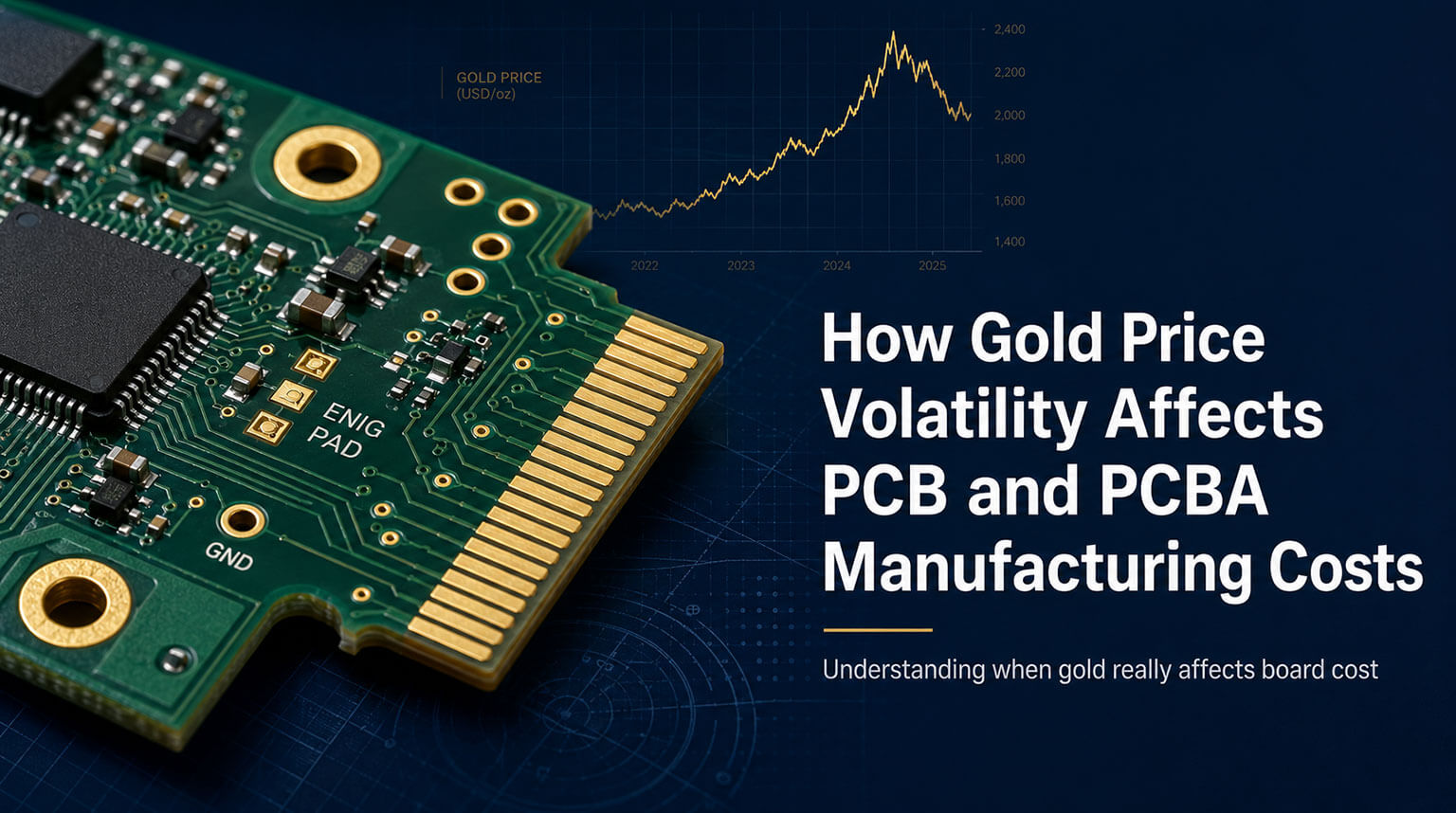
Gold price volatility is not usually the first thing a hardware team thinks about when reviewing a PCB quotation. However, in 2026, gold has become harder to ignore.
World Gold Council reported that the LBMA PM gold price reached a Q1 2026 quarterly average record of US$4,873/oz, with a historical high of US$5,405/oz in January before a correction later in the quarter. Reuters reported that gold was trading near US$3,969/oz on July 1 after its largest quarterly drop since 2013.
For PCB and PCBA buyers, the issue is not whether gold will rise or fall next. The real issue is whether a design uses enough gold for that volatility to matter.
The most useful way to discuss gold cost is not by saying “gold is expensive.” Everyone already knows that. The more useful question is:
How much gold is actually being deposited?
A simple approximation is:
Gold mass = plated area × gold thickness × gold density
Gold has a density of about 19.3 g/cm³, and one troy ounce equals 31.1034768 grams. Using a reference gold price of US$4,000/oz, one gram of gold is roughly US$128.6. That means 1 cm² of gold at 1 µm thickness contains about 0.00193 g of gold, worth about US$0.25 in raw metal value.
That number immediately explains why the cost is sometimes negligible and sometimes material.
These figures estimate only the theoretical raw gold value on the board. They are not PCB quotation prices. In real pricing, the surcharge must also cover nickel deposition, gold salt and plating chemistry…
As a practical reference, assuming the gold-plated area accounts for about 20% of the PCB area, PCBCool’s current ENIG surcharge is approximately US$32 per m² of PCB area for 1u” gold thickness, equivalent to about 0.025 µm, and approximately US$47 per m² of PCB area for 2u” gold thickness, equivalent to about 0.051 µm.
A common mistake is to put all “gold finish” choices into one bucket. From a cost and engineering perspective, ENIG and hard gold are very different.
ENIG uses a thin immersion gold layer over electroless nickel. IPC-4552B guidance is commonly associated with an immersion gold minimum around 0.05 µm and a typical range around 0.075–0.125 µm. The gold is thin because its main job is to protect the nickel surface before soldering and maintain solderability.
Hard gold is different. It is used where the surface is expected to experience repeated mating, sliding, wiping, insertion, or test contact. Gold fingers and edge connectors are typical examples. Industry guidance commonly places standard gold-finger thickness around 30–32 microinches, or about 0.76–0.81 µm, while high-reliability applications may require 50 microinches, or about 1.27 µm.
That means hard gold can easily use 10 times or more gold thickness than ENIG. If the plated area is also larger, the cost difference becomes much more than a surface-finish preference. It becomes a design economics question.
A gold chart moves every day. A PCB quotation does not.
This is one reason customers may be confused. Gold may fall in the market, but the PCB price may stay unchanged. Or gold may rise quickly, and a surcharge may appear in the next quote. The timing is not always symmetrical.
The reason is simple: PCB factories are not buying and selling gold like a trading desk. Gold enters the process through gold salts, plating chemistry, qualified baths, supplier inventory, and production scheduling. A factory may already have purchased chemical materials at a higher cost. A connector supplier may still be working through inventory bought before the pullback. A PCB shop may also shorten quote validity when precious-metal prices are unstable. Furthermore, as previously mentioned, the actual quote also includes a processing floor; consequently, for small-lot production, these fixed and semi-fixed costs can be more important than the metal value itself.
This is why gold volatility usually appears in PCB pricing through quote validity, surface-finish surcharge, order timing, and supplier communication, rather than through a simple one-to-one daily price adjustment.
Not every project needs a detailed gold-cost review. For a simple two-layer board with standard SMT assembly and limited ENIG area, it may not be worth over-analyzing. The review becomes more useful when gold has a functional role in the product.
Edge-card modules are the first category. If the board uses gold fingers, the cost depends directly on finger width, finger count, plated length, gold thickness, and order volume.
Industrial control products are another category. Many of these boards use replaceable modules, durable connectors, test contacts, or interfaces that must continue working after long field use.
RF and communication products also need careful review, but for a different reason. Gold may appear in RF connectors, contact areas, shielding interfaces, or selected surface finishes. At the same time, ENIG is not automatically the right finish for every RF area because the nickel layer can create performance concerns in some high-frequency designs. Cost and electrical performance need to be reviewed together.
Medical, automotive, aerospace-like, and other high-reliability electronics should be handled carefully. In these projects, removing gold only to reduce cost can create reliability risk. The better approach is to confirm where gold is technically required and where it may be a legacy specification that no longer matches the design.
The best time to control gold-related cost is before the fabrication drawing is frozen.
First, confirm whether ENIG is really required. If the board has fine-pitch BGAs, QFNs, dense SMT, long storage requirements, or multiple reflow cycles, ENIG may be the right choice. If the design is simple, the assembly window is short, and component pitch is not demanding, OSP, immersion silver, or lead-free HASL may be worth comparing.
Second, separate soldering surfaces from wear surfaces. ENIG may be suitable for solderable pads, but repeated mechanical contact usually requires hard gold. A mixed approach—hard gold only on fingers and another finish elsewhere—can often control cost without weakening the design.
Third, specify gold thickness clearly. “Gold finish” is not enough. The drawing should state whether the requirement is ENIG, ENEPIG, hard gold, or selective gold, and it should define the relevant thickness and plated area.
Fourth, reduce unnecessary plated area. In volume production, exposed copper area, connector geometry, selective plating strategy, and panel design can all affect total precious-metal consumption.
Fifth, review PCBA components for gold-plated contact exposure. Connector plating, mating-cycle requirements, contact force, environment, and expected service life should be checked before choosing heavy gold by default.
Finally, keep quotation timing aligned with production timing. In a volatile metal market, a quote issued for a prototype may not remain valid for mass production several months later. If the product uses ENIG, ENEPIG, hard gold, or gold-plated connectors, the quotation should state how long the price is valid and whether precious-metal surcharges may apply.
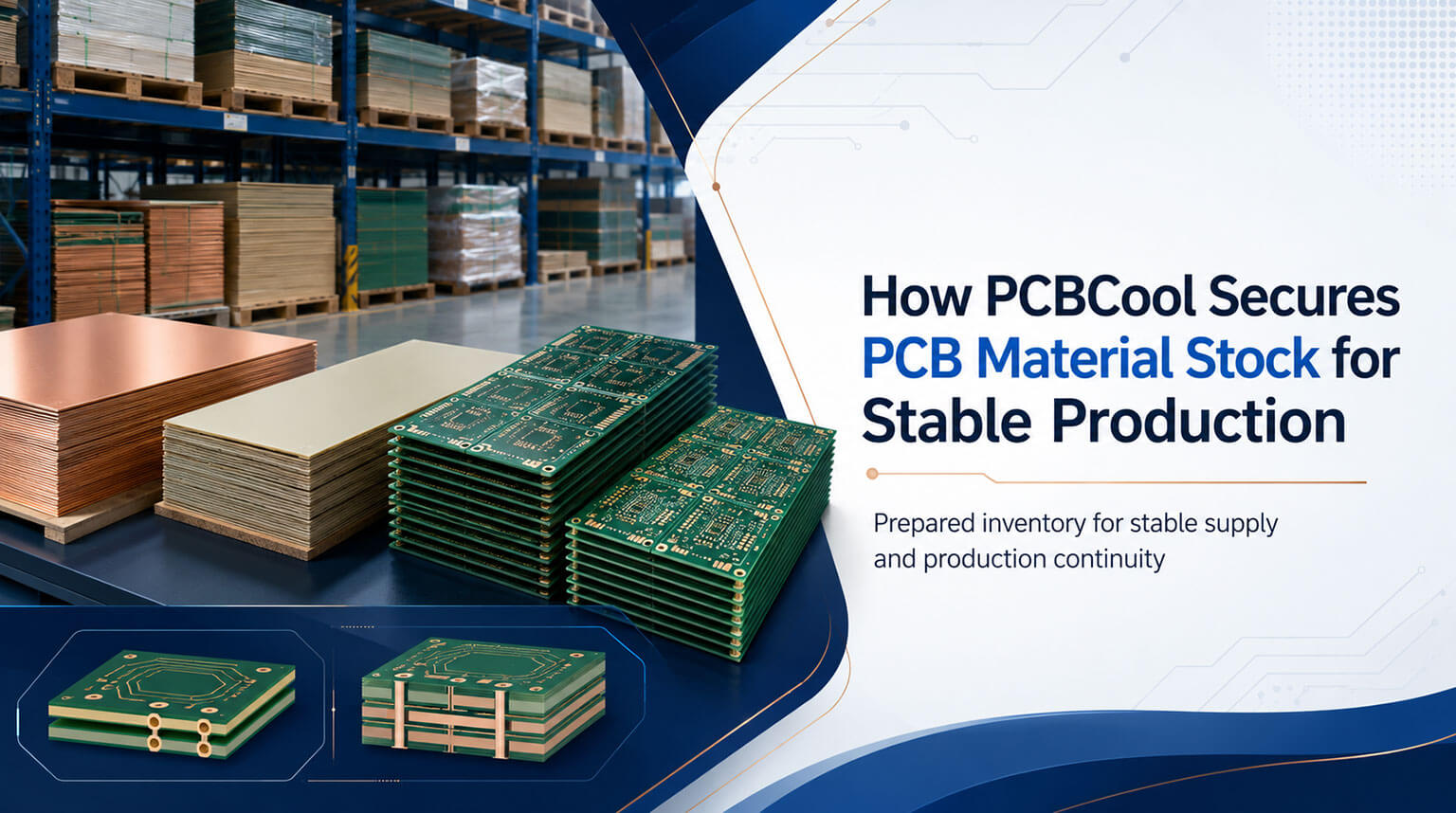
Gold price volatility is worth watching, but for most PCB projects, it is still a manageable cost factor rather than the biggest risk. Material shortages can create a much larger threat. The PCB industry saw this during the 2021 component shortage, and again during the 2026 PCB material shortage, when delayed supply affected not only cost but also production schedules.
This is why choosing the right PCB and PCBA partner matters. A recent example is how PCBCool prepared inventory ahead of the shortage: our team secured additional key substrate materials before supply pressure reached customers, helping reduce the risk of avoidable delays and production disruption.