If you’ve ever soldered, tinkered with DIY electronics, or taken apart devices like smartphones, headphones, or routers, you’ve probably seen those tiny, densely packed components on a circuit board—without long leads, sitting directly on the board surface, compact and precise. The core technology behind this is what we call SMT, which has revolutionized electronics manufacturing and is a key reason modern devices keep getting smaller and more powerful.
For electronics enthusiasts, understanding SMT not only helps you read circuit boards and master manual surface-mount soldering, but also allows your DIY projects to move from bulky to precise. This article breaks down SMT in a straightforward, easy-to-understand way—no heavy jargon, no overly technical deep dives—so you can grasp this essential electronic process.
SMT, short for Surface Mount Technology, is an assembly process where electronic components are directly mounted and soldered onto the surface of a printed circuit board (PCB).
To compare simply: before SMT became widespread, the electronics industry used THT (Through-Hole Technology). Components had long metal leads that needed to pass through holes in the PCB and be soldered from the other side. SMT eliminates the “through-hole” step: components are mounted directly on the PCB surface, and soldering is done on the same side. This shift ushered in the era of miniaturized electronics.
In short, without SMT, there would be no ultra-thin smartphones, portable headphones, or mini smart devices.
Like any technology, SMT was developed to solve real-world problems. Its evolution mirrors the upgrades in the electronics industry over decades.
As early as the 1960s, electronic devices still used THT technology. Components were large and assembly was slow, making it impossible to meet the demand for smaller electronic products. The military and aerospace sectors first pushed for miniaturization and lightweight designs, driving the development of new assembly techniques. This was the birth of SMT.
In the 1970s and 1980s, consumer electronics began to rise—TVs and radios became widespread—and the limitations of traditional THT became more evident. SMT entered a rapid development phase, with specialized surface-mount components and soldering equipment gradually emerging. By the 1990s, portable electronics like mobile phones and computers exploded onto the market, and SMT completely replaced THT, becoming the industry standard.
In the 21st century, with the rise of smartphones, IoT devices, and smart hardware, SMT has continued to evolve. From early manual placement and simple soldering, it has developed into fully automated high-speed placement and intelligent reflow soldering, greatly improving assembly precision and efficiency. This has driven electronics toward being thinner, more precise, and smarter.
The components used in SMT are collectively called SMDs (Surface-Mount Devices). They differ significantly in shape from traditional through-hole parts and cover a wide range of electronic needs:
- Passive Components: Basic chip resistors, capacitors, and inductors. Usually small square packages with no polarity, tiny in size.
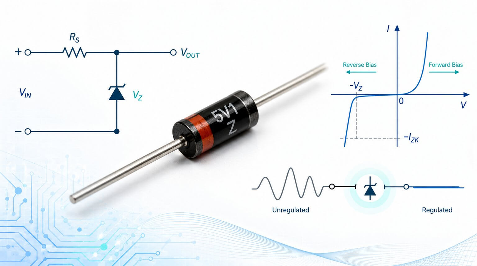
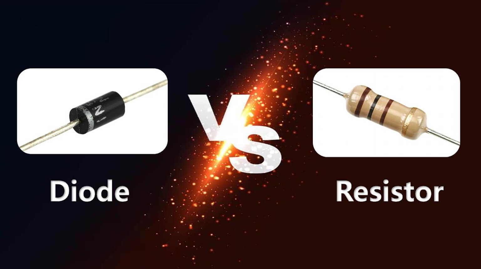
- Discrete Semiconductors: Chip diodes, transistors, and FETs. These have one-way conductivity or signal amplification functions, with clearly defined leads and polarity.
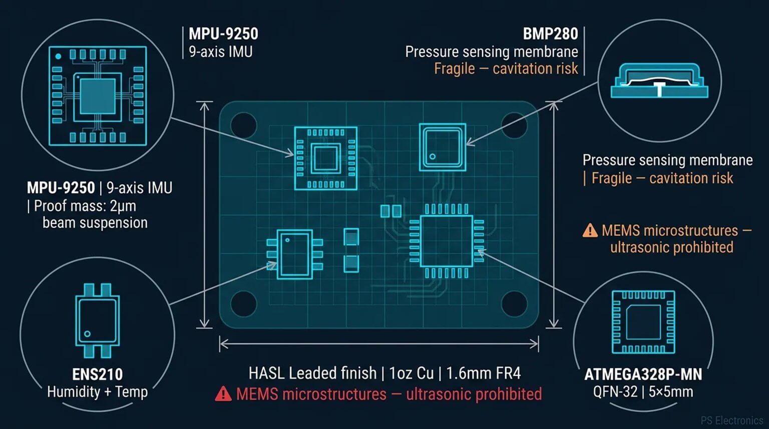
- Integrated Circuits (ICs): Microcontrollers, voltage regulators, memory chips, etc. Come in various packages such as SOIC, QFP, QFN, with dense pins, serving as the core control units of circuits.
- Special-Shaped Components: Chip LEDs, connectors, USB ports, buttons—used for interfaces, displays, or user operations, all compatible with SMT assembly.
SMT requires specialized equipment, which differs between industrial mass production and DIY enthusiasts, but serves the same core purpose:
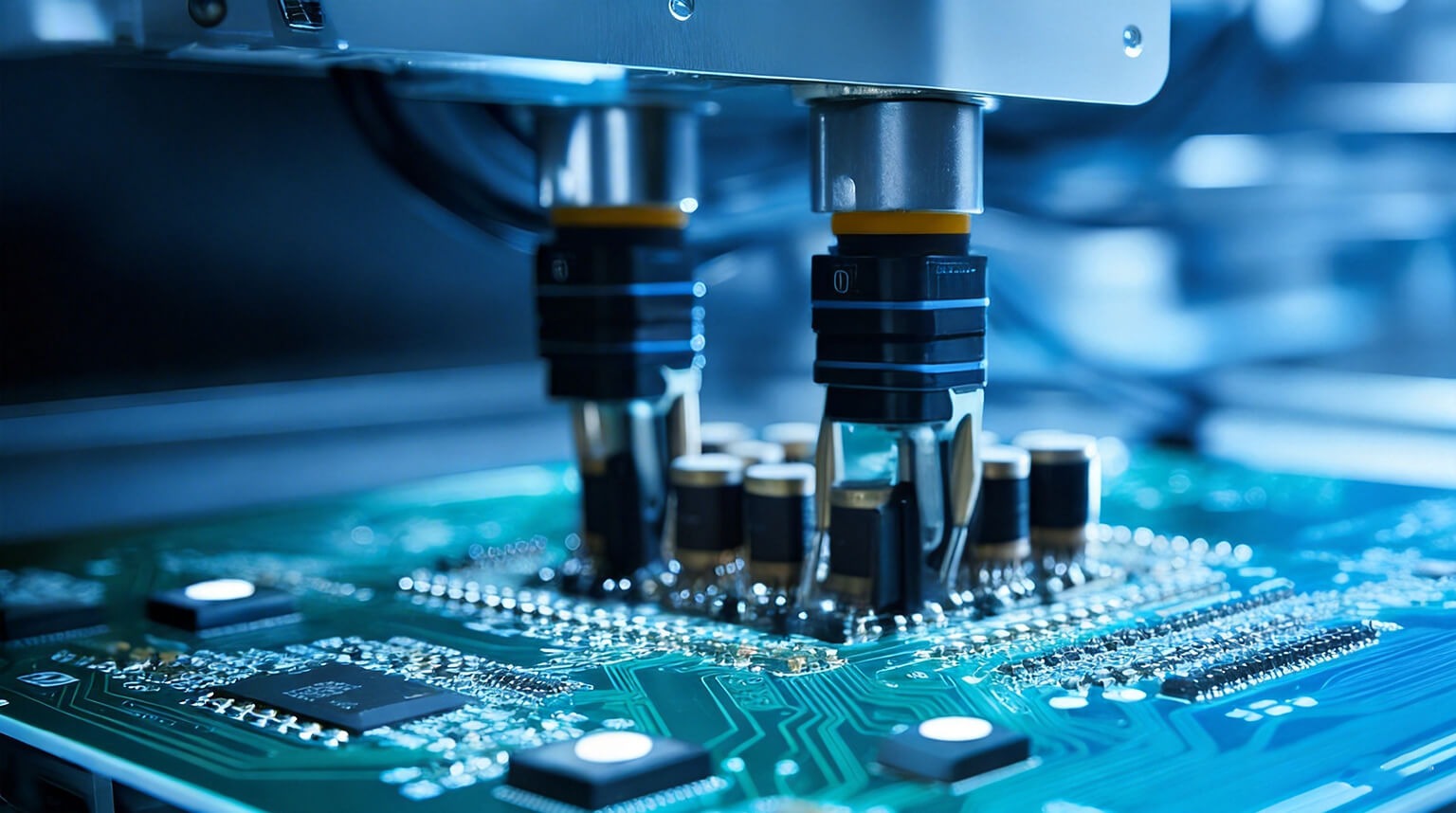
- Industrial Equipment: Solder paste printer, high-speed pick-and-place machines, reflow soldering ovens, AOI (Automated Optical Inspection) systems, repair stations.
- DIY Tools for Enthusiasts: Temperature-controlled soldering irons, hot air guns, anti-static tweezers, solder flux, desoldering braid, anti-static wrist straps.
SMT became the industry mainstream because it solved many pain points of traditional THT. Its core advantages are:
- Miniaturization: SMDs have no long leads and are extremely small (common 0402, 0603 packages are smaller than a fingernail). This drastically reduces PCB space, making devices more compact and refined.
- High Assembly Density: On the same size PCB, SMT can accommodate multiple times the number of components compared to THT, increasing PCB utilization. Small boards can now achieve multiple functions, such as mini development boards or micro sensor modules.
- Better High-Frequency Performance: Short leads reduce signal interference and loss, ideal for RF, wireless, and high-frequency circuits—why routers, Bluetooth devices, and similar electronics use SMT.
- Higher Reliability: Components sit firmly on the PCB surface, solder joints are strong, resistant to vibration and shocks—important for automotive electronics or outdoor devices.
- Automation-Friendly: Industrial production can achieve fully automated assembly lines—placement, soldering, and inspection all in one. Even DIY assembly is simplified and faster.
- Reduced Material Waste: No need for numerous drilled holes, less PCB material wasted, components consume less material, and overall costs are reduced.
Although SMT has obvious advantages, it is not perfect. Both hobbyists and industrial producers face some challenges:
- Higher Difficulty for Manual Soldering: Ultra-small packages like 0402 or dense-pin ICs like QFP/QFN are difficult to align manually, increasing the risk of cold solder joints or solder bridges.
- Components Are Fragile and Hard to Replace: SMDs are tiny and easily damaged. Mistakes during soldering make removal and repair tricky, risking damage to the component or PCB pads.
- Strict Anti-Static Requirements: Dense ICs and chips are highly susceptible to electrostatic discharge. Proper anti-static measures are essential, or components can be permanently damaged.
- High Repair Costs: Industrial rework requires specialized equipment. Manual repair is technically demanding, and troubleshooting complex packages is challenging.
- High Precision Requirements: Slight misalignment in solder paste printing or component placement can compromise solder quality and cause circuit failures.
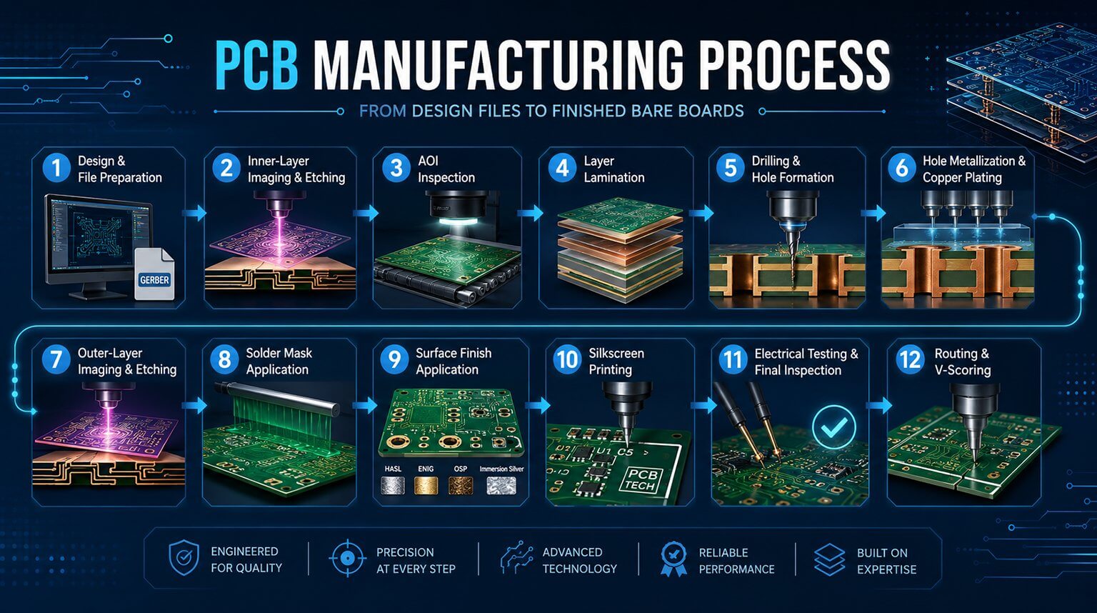
Whether for industrial mass production or DIY prototyping, the core workflow of SMT is consistent and can be summarized in five clear steps:
- Solder Paste Printing
The first step in SMT is applying solder paste to PCB pads through a stencil. This acts as a “primer” for soldering, ensuring components will adhere firmly. Industrial production uses fully automated printers, while hobbyists can scrape paste manually.
- Komponentenplatzierung
Place SMD components precisely onto the printed solder paste. Industrial lines rely on high-speed pick-and-place machines with millisecond-level accuracy. Hobbyists use anti-static tweezers with magnifying tools for manual alignment.
- Reflow-Löten
Send the PCB with components into a reflow oven, passing through preheating, soaking, reflow, and cooling stages. The solder paste solidifies, firmly attaching components to the PCB. Hobbyists can use small reflow stations or hot air guns to achieve the same result.
- Quality Inspection
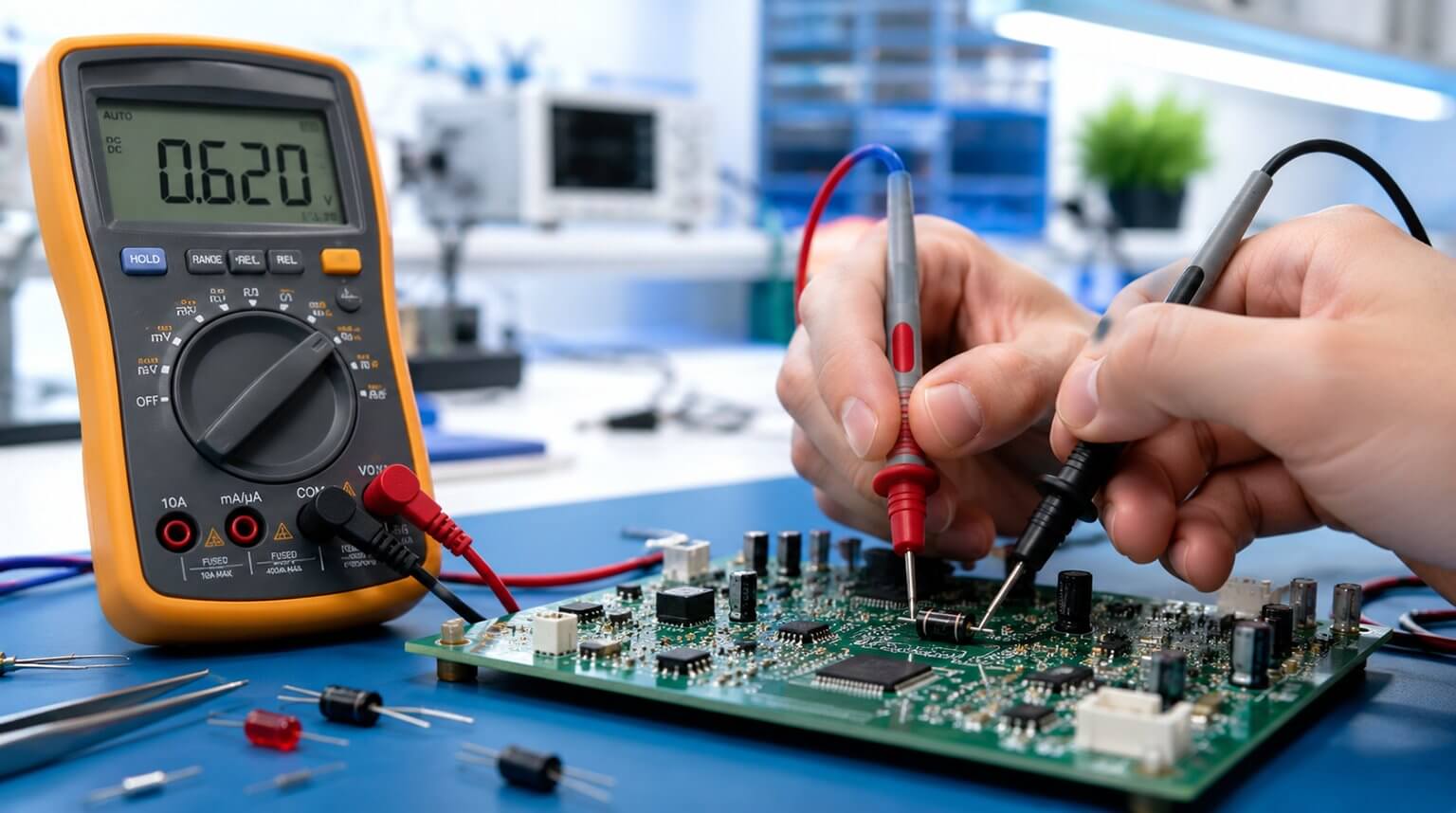
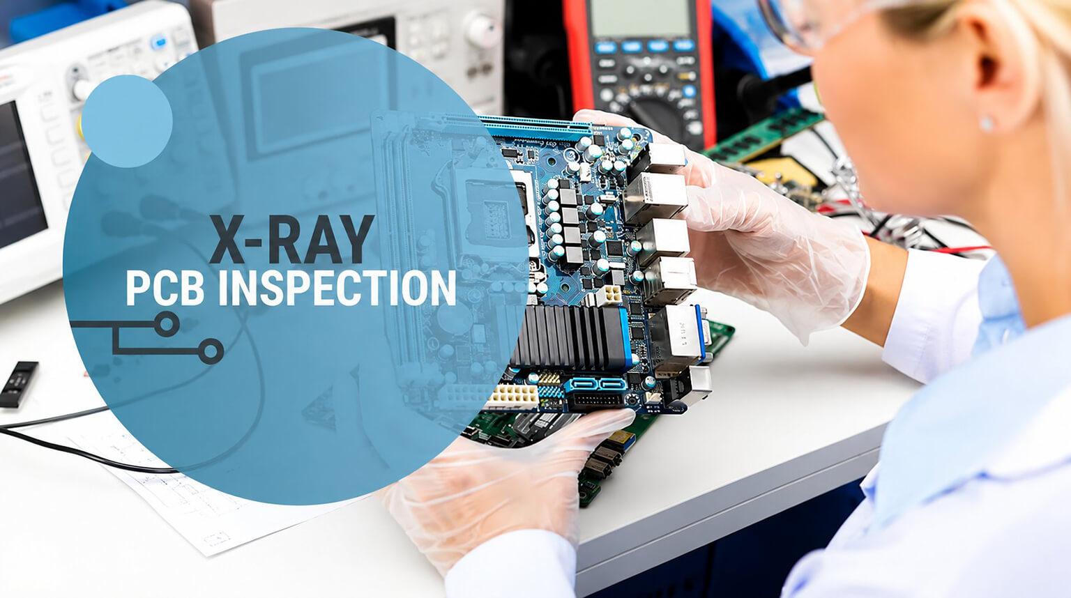
After soldering, check for cold joints, solder bridges, misaligned or missing components. Industrial lines use AOI machines for automated scanning. Hobbyists can visually inspect with a magnifying lens and use a multimeter to test continuity.
- Rework and Cleaning
Repair any defective solder joints using desoldering braid or hot air guns for cold joints. Finally, clean residual flux from the PCB to prevent corrosion and ensure product stability.
Although SMT may seem like an industrial process, it is also a crucial skill for electronics enthusiasts. It allows devices to break free from bulky constraints, achieving a perfect balance between compact size and powerful functionality. Whether you’re creating DIY projects, repairing electronics, or exploring hardware fundamentals, understanding SMT helps you see deeper, solder smarter, and build more professional projects.
Bei PCBCool, we make working with SMT easier than ever. We offer high-quality SMT PCB bare boards for your designs, as well as full SMT assembly services for both prototyping and production. Whether you are an enterprise looking for reliable manufacturing solutions or a hobbyist seeking precise DIY support, PCBCool provides the tools and expertise to bring your electronic projects to life.