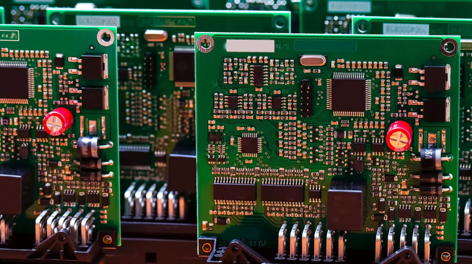
Printed circuit boards (PCBs) are almost everywhere in electronic devices—they form the foundation that allows all electronics to function properly. But once you actually step into this field, you’ll quickly realize that making a PCB is not as simple as just “manufacturing it.”
You might hear a variety of related terms—PCB fabrication, PCB assembly, mass production, prototyping…
Many beginners initially think: “Isn’t it just making the board? Why are there so many steps?”
In reality, every stage from design to final mass production is crucial. Skipping any step can lead to unstable performance, or even prevent a product from successfully reaching the market.
In diesem Artikel, PCBCool will give you a full picture of PCB prototyping and explain why it is indispensable.
In simple terms, PCB prototyping is the process of producing a small batch of boards (usually 1–10 pieces) based on your designed schematics to verify whether your design actually works.
These prototype boards are not meant for final products; instead, they are used for various tests, such as checking electrical performance, confirming functionality, and detecting design issues early.
In other words, prototyping is like a “trial run” before mass production. Its purpose is not to produce but to validate.
At its core, the main goal of prototyping is straightforward: to verify that your design really works.
Some beginner engineers often think:
“I followed the tutorial step by step, double-checked everything, and ran a DRC (Design Rule Check). It should be fine, right?”
It sounds reasonable, but reality is often more complicated.
First, it’s important to understand that DRC does not equal ‘correct design.’
Rules are set by you and may not always reflect what’s truly reasonable.
For example:
- You might set a 0.25 mm spacing rule, but certain power circuits actually require larger safety margins.
- Your design may include high-speed signals but lacks impedance control—DRC won’t catch this.
More importantly, DRC only checks whether rules are followed; it cannot cover real-world issues, such as:
- Signal integrity (SI) problems
- Power integrity (PI) issues
- EMI/EMC interference
- Crosstalk or reflections at high frequencies
In actual electronic products, there are many “non-ideal factors,” such as soldering quality, component tolerances, PCB warpage, or even mechanical interference from connectors.
These problems are hard to fully expose in software simulations, but in real production, they can be amplified dramatically.
This is why PCB prototyping is so critical—it helps you “walk through the pitfalls” before mass production.
From a cost perspective, prototyping is also worthwhile:
- A standard computer motherboard might cost $8 per piece in mass production; producing 1,000 pieces costs $8,000.
- In the prototype stage, the unit price might be $80, and making 5 boards only costs $400.
If you detect issues during prototyping, you can fix your design at a minimal cost. But if you skip this step and go straight to mass production, mistakes can lead to multiplied or even irrecoverable losses.
So rather than seeing prototyping as an extra step, it is actually the most cost-effective form of insurance in the entire PCB development process.
You might be surprised: the unit price for a prototype PCB is much higher than mass production.
While exact numbers vary by project, in practice prototype boards are often 5–10 times more expensive per piece than mass-produced ones. This is not an exaggeration.
Why is that? After all, the same manufacturer is handling the same design.
There are two main reasons:
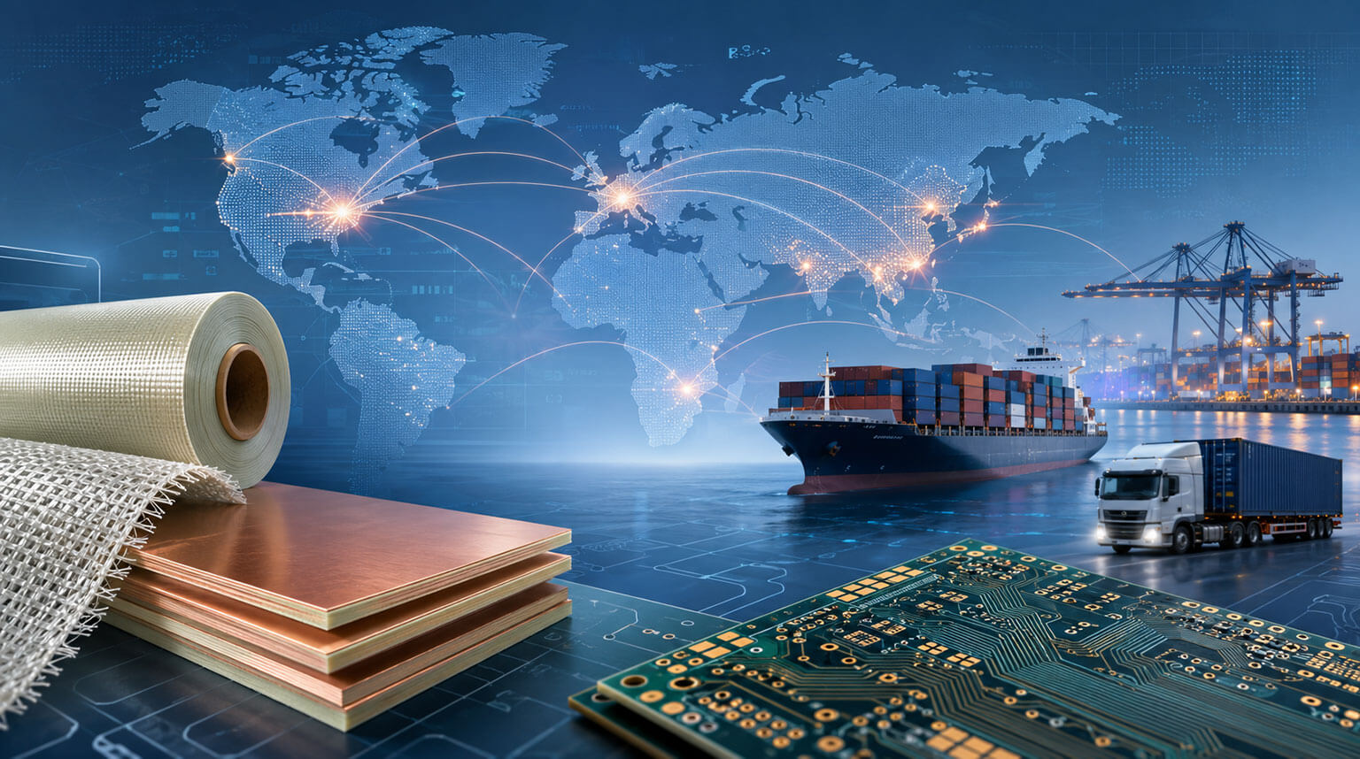
1. Panel Utilization Effect
PCB fabrication usually involves “panelization,” meaning multiple small boards are arranged on a single large panel for processing.
In mass production, large orders allow full utilization of the panel, so every inch of material is used efficiently, lowering the unit cost.
In prototyping, you might only need 5 boards.
However, the machinery has a fixed processing area, and the factory still needs to operate at a “minimum production area.”
In other words, you only use a small portion of the panel but must pay for the entire panel—this drives up the unit price.
2. Fixed Setup Costs Cannot Be Spread
PCB production is not as simple as pressing a button.
From engineering preparation, film production, and equipment calibration to actual operation, each step requires time and cost.
For large orders, these costs are distributed across hundreds or thousands of boards, making them negligible per unit.
For prototype orders, the fixed costs must be absorbed by only a few boards.
Additionally, small prototype orders may disrupt the factory’s existing schedule, causing extra costs that appear in quotes.
In short, prototype PCB are expensive because you are using near-mass-production processes without the scale of mass production, and therefore lose cost advantages.
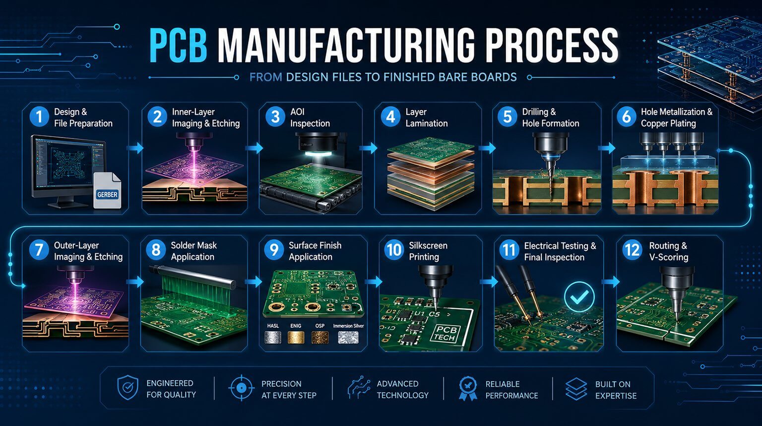
The essence of prototyping is still to turn your design into a tangible circuit board you can hold in your hands. The process can be broken down into several key steps:
- Preparing Design Files
Before contacting a manufacturer, you need to complete your PCB design and export standard production files (usually Gerber files).
If you lack design skills, you can also choose a “turnkey PCB assembly service,” where the manufacturer handles everything from design to finished product.
- Ingenieurwesen-Rundschau
Once the manufacturer receives your files, engineers typically review them, checking:
- Whether the routing is reasonable
- Drill hole sizes and manufacturability
- Trace width and spacing compliance with process requirements
- Component footprint compatibility
An experienced team may also offer optimization suggestions, such as adjusting spacing or improving hole placement.
The core goal of this step is simple: ensure that your design can actually be manufactured.
- Material Preparation and Cutting
After the design is approved, the factory selects the appropriate base material and cuts it to the required size in preparation for processing.
- Circuit Patterning
This is one of the most critical steps in PCB manufacturing.
Simply put, it’s the process of “printing” the designed circuit onto the board:
- Copper is laminated onto the substrate
- Unnecessary copper is removed using photolithography and etching, leaving the designed circuit intact
For multilayer boards, layers are then laminated together to form the full stack.
- Drilling and Via Processing
Holes are drilled on the PCB for:
- Through-hole components (like DIP)
- Electrical connections between layers
CNC drilling is standard, while laser drilling may be used for high-precision or fast-turn requirements.
- Solder Mask and Silkscreen
The green layer commonly seen on PCBs is the solder mask, which protects circuits and prevents short circuits.
On top of the solder mask, silkscreen (white markings) is printed to indicate component locations and parameters.
- Component Assembly
If your prototype includes components (PCBA), assembly comes next:
Components are soldered onto the PCB using SMT, reflow soldering, and related processes.
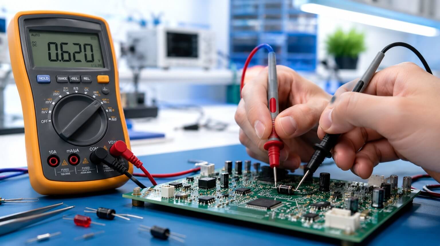
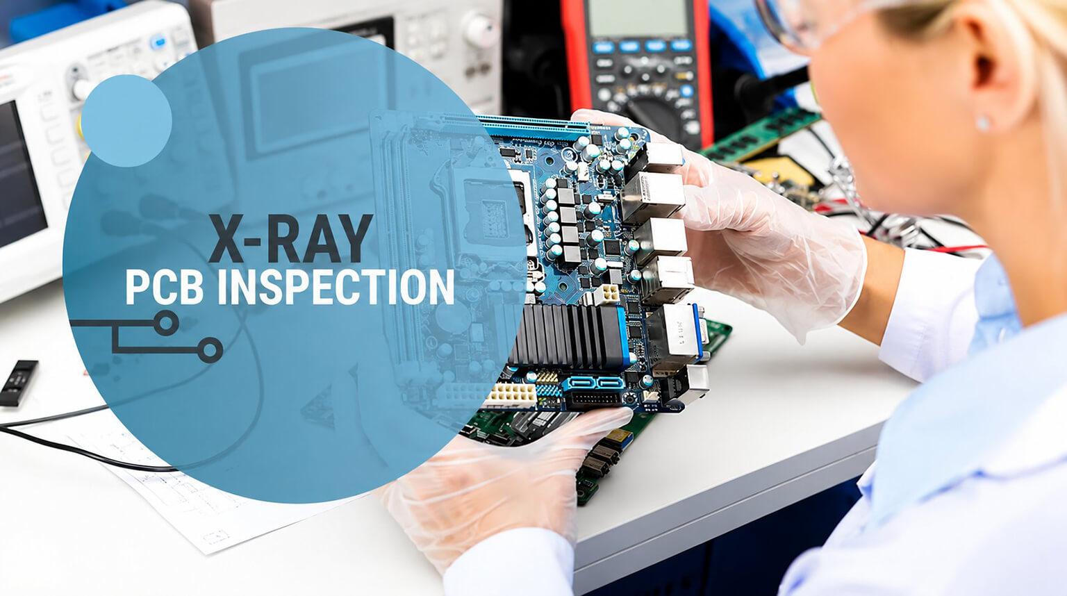
- Testing and Validation
The final step—and the main purpose of prototyping—is testing:
- Electrical performance (signals, voltage, current)
- Mechanical fit (soldering strength, dimensional accuracy)
- Design issues (short circuits, open circuits, interference)
- Iterative Optimization
If problems are found, the design is revised and the board is re-prototyped.
This cycle repeats:
Design → Prototype → Test → Revise → Prototype again
Only when the product fully meets expectations is the prototyping stage considered complete.
PCB prototyping may seem like just “making a few sample boards,” but its real significance lies in turning designs on a screen into tangible products that can be validated, corrected, and eventually mass-produced.
For beginners, prototyping is the critical step from “being able to draw a schematic” to “being able to make a product.”
For companies, it is a key way to control risk, optimize costs, and accelerate product launch.
Bei PCBCool, we serve both professional electronics engineering teams and hobbyists or startups. Whether you have just completed your first PCB design or are working on complex industrial PCB projects, we provide reliable, high-quality prototyping services.
For long-term commercial partners, we even offer free prototype boards to help reduce trial-and-error costs during early development and speed up project progress.
If you are about to start your next PCB design, why not begin with a high-quality prototype?