Nowadays, electronic products, especially smartphones and laptops, are becoming increasingly focused on being lightweight and slim. Many brands even make “light” and “thin” their key selling points. Behind this trend, there is an important “unsung hero” that is always indispensable—Flexible Leiterplatte.
If you’re new to the electronics field or not familiar with flexible PCB, this beginner’s guide is perfect for you. PCBCool will take you through all the core concepts of flexible PCB, and even without diving into the technical details, you’ll be able to grasp the essentials.
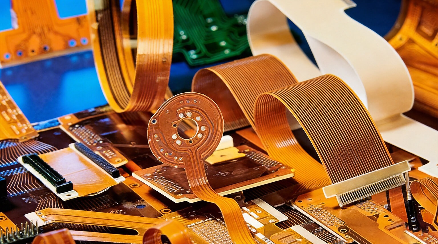
A flexible PCB, abbreviated as FPC, is a type of circuit board based on flexible insulating materials. It can bend, fold, and roll, offering a unique advantage in many applications. By etching conductive circuits on the material’s surface, a flexible PCB can act as a bridge connecting two rigid PCB (rigid-flex PCB) or, by mounting electronic components, serve various functions.
Compared to traditional rigid boards (like those used in computer motherboards or routers), the biggest advantage of flexible PCB is their outstanding adaptability. They can bend or fold according to the device’s structural requirements, greatly saving space and reducing weight, thus helping to design lighter and more compact electronic products.
The substrate is the “skeleton” of the flexible PCB and is key to its flexibility. It needs to be insulating, flexible, and heat-resistant. Common materials for flexible PCB substrates include Polyimide (PI), Polyester (PET), and Polyethylene Naphthalate (PEN).
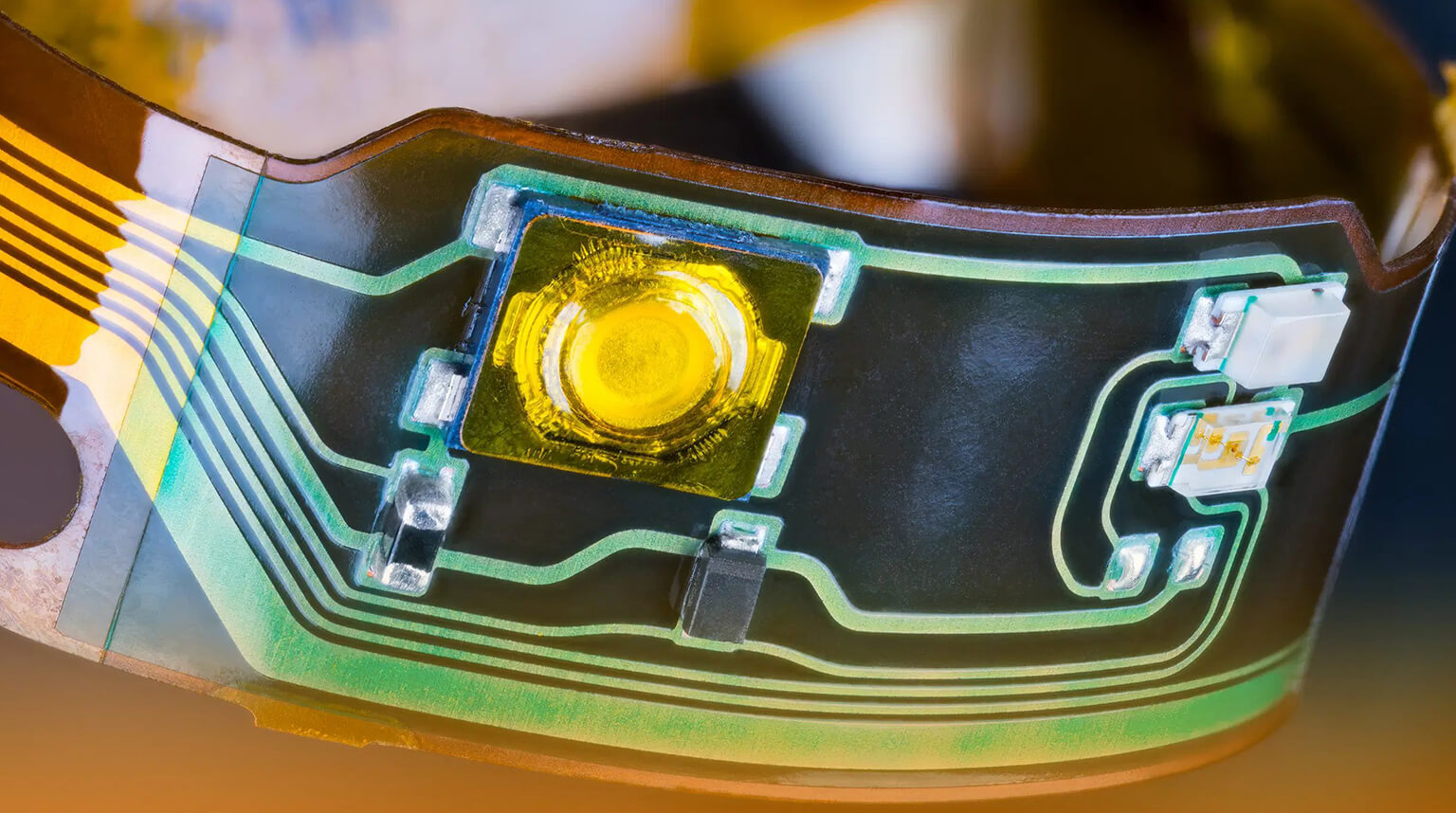
The conductive layer is created by etching to form predefined circuit patterns, responsible for connecting the pins of various components. It is the core part that enables electrical signal and power transmission. The copper foil used in flexible PCB is typically electrolytic copper foil or rolled copper foil.
The cover layer acts as a “protective layer” for the flexible PCB, covering the conductive layer’s surface. Its main role is to prevent oxidation, wear, and to shield the PCB from dust and moisture, while also enhancing the mechanical strength of the PCB. This layer can be made from a cover film or solder mask ink.
The adhesive layer is used to connect the substrate, conductive layer, and cover layer, ensuring that these layers remain tightly bonded and do not delaminate or peel off. Common adhesive materials include acrylic adhesive and epoxy resin adhesive.
Since flexible PCB are generally thin and soft, reinforcing layers are often added in areas where components (like chips or connectors) need to be soldered or fixed. These reinforcement layers help provide localized strengthening, making it easier to solder and preventing heat damage to the substrate. Common materials for reinforcing layers include FR-4, PI boards, and steel sheets.
- Pads: The exposed parts of the conductive layer used for soldering electronic components. These are the connection points between the components and the circuits.
- Gold Fingers: Some flexible PCB feature gold-plated connectors (called “gold fingers”) at the ports. These are used for inserting interfaces (such as graphics cards, memory sticks), enhancing conductivity and wear resistance.
- Marking Layer: The printed text or symbols on the PCB surface (such as part numbers, direction markers) that assist in production, soldering, and maintenance.
Flexible PCB can be categorized based on the number of circuit layers and structural complexity:
- Single-Sided: Contains only one conductive layer. It is the simplest structure with the lowest cost, with the circuitry arranged on just one side. This is suitable for simple signal transmission and is commonly used in toys, basic sensor connections, etc.
- Double-Sided: Has two conductive layers, one on each side of the substrate. The two layers are connected via vias. This is suitable for devices with moderate complexity, such as standard smartwatches, headphones, etc.
- Multilayer: Has four or more conductive layers, connected through vias. This structure is more complex and precise, supporting more components and intricate circuits. It is commonly used in high-end devices like smartphones, foldable screens, aerospace equipment, etc.
- Rigid-Flex: Combines both flexible and rigid parts. The flexible portion is used for bending and fitting, while the rigid part is for securing components and enhancing stability. This is widely used in smartphone camera modules, automotive electronics, medical devices, and more.
Flexible PCB can also be categorized based on application scenarios and features:
- Transparent: Made using transparent substrates and conductive layers, avoiding the visibility issues common with traditional PCB materials. These are used in applications like flexible transparent displays, wearable devices with transparent panels, and automotive transparent displays.
- Streifen Designed as a long strip, the circuit structure is similar to regular flexible PCB. These are commonly used in LED projects, where the circuit structure is relatively simple, often employing single-layer or double-layer configurations.
- Thin: Typically thinner than 0.1mm, made from ultra-thin PI and copper foil. These are very lightweight and flexible, making them ideal for tight, precise device structures. They are widely used in medical micro-implantable devices.
Compared to traditional PCB manufacturing, the process of making flexible PCB is more complex and challenging, but the core steps are generally similar. Here’s an overview of the key steps, from raw materials to finished product:
- Substrate Preparation: Choose an appropriate flexible substrate (such as PI), and cut it into the required size.
- Conductive Layer Lamination: Attach copper foil to the surface of the substrate using an adhesive layer, creating a “copper foil substrate.”
- Circuit Etching: Apply photoresist to the copper foil, expose and develop it to reveal the desired circuit pattern. Then, use an etching process to remove the excess copper foil, leaving behind the pre-designed circuits.
- Cover Layer Lamination/Solder Mask Printing: Apply a cover film or print a solder mask ink over the conductive layer, protecting the circuits and exposing the pads.
- Reinforcing Layer Lamination: In areas requiring reinforcement (such as pads or connectors), add the reinforcement layer to provide local strengthening.
- Surface Treatment: Perform surface treatments on pads and gold fingers (such as gold plating or tin plating) to enhance conductivity and wear resistance.
- Shaping and Cutting: Cut the PCB into the final shape, removing excess material.
- Testing and Inspection: Check the conductivity, insulation, and flexibility of the circuit to ensure the product is qualified and free of issues like short circuits or open circuits.
The future of electronics is headed toward lightweight and intelligent devices, which reflects the growing importance of flexible circuits. Based on the future trends in electronic products, the development of flexible PCB is also becoming increasingly clear:
- Thinner Designs: By enhancing processing capabilities for flexible substrates and copper foil, the production of even thinner flexible PCB is becoming possible.
- Higher Density: As circuits get finer, drilling becomes more miniature, and even smaller volumes can achieve the same functionality.
- Increased Reliability: Especially for flexible PCB that undergo dynamic bending, the number of bending cycles before failure continues to increase.
- Cost Reduction: With advances in technology and mass production, the cost of flexible PCB is gradually decreasing, expanding their application range.
- Enhanced Special Properties: Capabilities like high-temperature resistance, waterproofing, and high-frequency transmission are continuously improving, allowing flexible PCB to adapt to more extreme environments and high-end needs.
- Rigid-Flex PCB Becomes Mainstream: Rigid-flex PCB combine the flexibility of the flexible portion and the stability of the rigid section, making them widely applicable in high-end devices.
In short, flexible PCB are circuit boards that maintain electrical functionality even when bent or folded. They address the limitations of rigid PCB, making them ideal for applications in complex structures and miniaturized devices.
If you have more questions or would like to discuss flexible PCB in further detail, feel free to reach out to us. If you’re considering outsourcing your flexible PCB manufacturing and assembly, PCBCool is here to help. We offer manufacturing capabilities for flexible PCB with 1 to 6 layers, as well as assembly capabilities for fine-pitch components like BGA and SMD. We can provide a one-stop solution for all your project needs.